SCAS339U March 1994 – July 2024 SN74LVC126A
PRODUCTION DATA
4 Pin Configuration and Functions
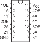
 Figure 4-1 SN74LVC126A D, DB, DGV, NS, or PW Package;14-Pin SOIC, SSOP, TVSOP, SOP or TSSOP
(Top View)
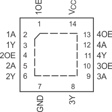
 Figure 4-2 SN74LVC126A BQA or RGY Package;14-Pin WQFN or VQFN
(Top View)
Figure 4-2 SN74LVC126A BQA or RGY Package;14-Pin WQFN or VQFN
(Top View)Table 4-1 Pin Functions
| PIN | I/O(1) | DESCRIPTION | |
|---|---|---|---|
| NO. | NAME | ||
| 1 | 1OE | I | Output enable 1 |
| 2 | 1A | I | Gate 1 input |
| 3 | 1Y | O | Gate 1 output |
| 4 | 2OE | I | Output enable 2 |
| 5 | 2A | I | Gate 2 input |
| 6 | 2Y | O | Gate 2 output |
| 7 | GND | — | Ground pin |
| 8 | 3Y | O | Gate 3 output |
| 9 | 3A | I | Gate 3 input |
| 10 | 3OE | I | Output enable 3 |
| 11 | 4Y | O | Gate 4 output |
| 12 | 4A | I | Gate 4 input |
| 13 | 4OE | I | Output Enable 4 |
| 14 | VCC | — | Power pin |
| Thermal pad | — | Connect the GND pin to the exposed thermal pad for correct operation. Connect the thermal pad to any internal PCB ground plane using multiple vias for good thermal performance. | |
(1) I = input, O = output, P = power,
FB = feedback, GND = ground, N/A = not applicable