SCAS523E October 2003 – July 2024 SN54ACT00 , SN74ACT00
PRODUCTION DATA
3 Pin Configuration and Functions
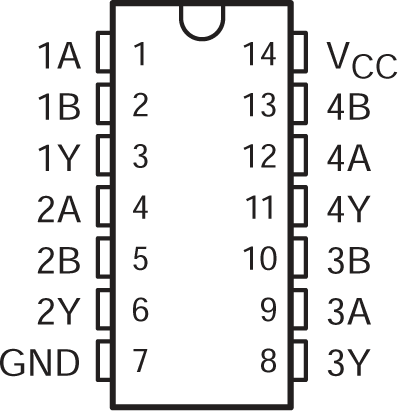
 Figure 3-1 SN54ACT00 J or W Package; SN74ACT00
D, DB, N, NS, or PW Package (Top View)
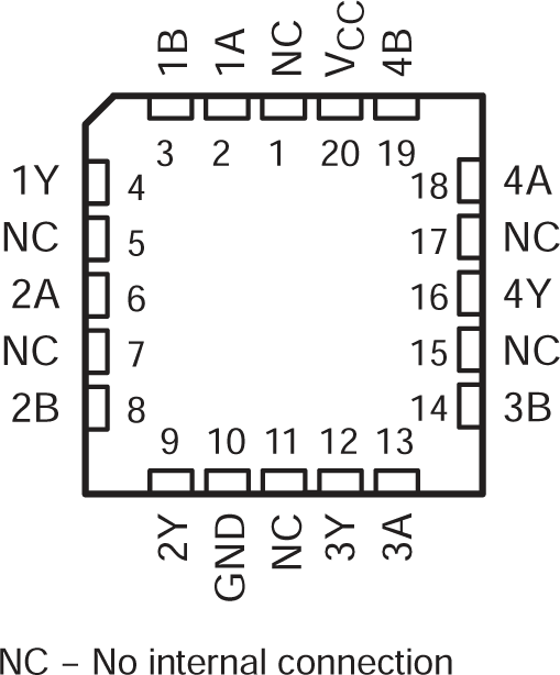
 Figure 3-2 SN54ACT00 FK Package (Top View)
Table 3-1 Pin Functions
| PIN | TYPE(1) | DESCRIPTION | |
|---|---|---|---|
| NAME | NO. | ||
| 1A | 1 | I | Channel 1, Input A |
| 1B | 2 | I | Channel 1, Input B |
| 1Y | 3 | O | Channel 1, Output Y |
| 2A | 4 | I | Channel 2, Input A |
| 2B | 5 | I | Channel 2, Input B |
| 2Y | 6 | O | Channel 2, Output Y |
| 3A | 9 | O | Channel 3, Output Y |
| 3B | 10 | I | Channel 3, Input A |
| 3Y | 8 | I | Channel 3, Input B |
| 4A | 12 | O | Channel 4, Output Y |
| 4B | 13 | I | Channel 4, Input A |
| 4Y | 11 | I | Channel 4, Input B |
| GND | 7 | G | Ground |
| VCC | 14 | P | Positive Supply |
(1) Signal Types: I = Input, O = Output, I/O
= Input or Output, P = Power Supply, G = Ground.