SCAS524F August   1995  – July 2024 SN54AC00 , SN74AC00

PRODUCTION DATA  
  1.   1
  2. Features
  3. Description
  4. Pin Configuration and Functions
  5. Specifications
    1. 4.1 Absolute Maximum Ratings
    2. 4.2 Recommended Operating Conditions
    3. 4.3 Thermal Information
    4. 4.4 Electrical Characteristics
    5. 4.5 Switching Characteristics: VCC = 3.3 V ± 0.3 V
    6. 4.6 Switching Characteristics: VCC = 5 V ± 0.5 V
    7. 4.7 Operating Characteristics
  6. Parameter Measurement Information
  7. Detailed Description
    1. 6.1 Functional Block Diagram
    2. 6.2 Device Functional Modes
  8. Application and Implementation
    1. 7.1 Power Supply Recommendations
    2. 7.2 Layout
      1. 7.2.1 Layout Guidelines
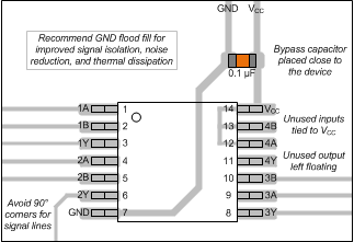
      2. 7.2.2 Layout Example
  9. Device and Documentation Support
    1. 8.1 Documentation Support (Analog)
      1. 8.1.1 Related Documentation
    2. 8.2 Receiving Notification of Documentation Updates
    3. 8.3 Support Resources
    4. 8.4 Trademarks
    5. 8.5 Electrostatic Discharge Caution
    6. 8.6 Glossary
  10. Revision History
  11. 10Mechanical, Packaging, and Orderable Information

Layout Example

SN54AC00 SN74AC00 Layout Example for the SNx4AC00 Figure 7-1 Layout Example for the SNx4AC00