SCAS526D August 1995 – July 2024 SN54ACT10 , SN74ACT10
PRODUCTION DATA
2 Description
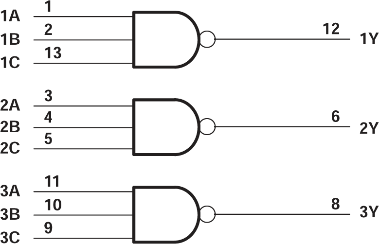
The ’ACT10 devices contain three independent 3-input NAND gates. The devices perform the Boolean functions Y = A • B • C or Y = A + B + C in positive logic.
Device Information
| PART NUMBER | PACKAGE(1) | PACKAGE SIZE(2) | BODY SIZE(3) |
|---|---|---|---|
| SNx4ACT10 | D (SOIC, 14) | 8.65mm × 6mm | 8.65mm × 3.9mm |
| N (PDIP, 14) | 19.3mm × 9.4mm | 19.3mm × 6.35mm | |
| DB (SSOP, 14) | 6.2mm x 7.8mm | 6.2mm x 5.3mm | |
| PW (TSSOP, 14) | 5mm × 6.4mm | 5mm × 4.4mm |
(1) For more information, see Mechanical, Packaging, and Orderable
Information.
(2) The package size (length × width)
is a nominal value and includes pins, where applicable.
(3) The body size (length × width) is
a nominal value and does not include pins.
 Logic Diagram, Each Gate (Positive
Logic)