SCAS526D August   1995  – July 2024 SN54ACT10 , SN74ACT10

PRODUCTION DATA  

  1.   1
  2. Features
  3. Description
  4. Pin Configuration and Functions
  5. Specifications
    1. 4.1 Absolute Maximum Ratings
    2. 4.2 Recommended Operating Conditions
    3. 4.3 Thermal Information
    4. 4.4 Electrical Characteristics
    5. 4.5 Switching Characteristics
    6. 4.6 Operating Characteristics
  6. Parameter Measurement Information
  7. Detailed Description
    1. 6.1 Functional Block Diagram
    2. 6.2 Device Functional Modes
  8. Application and Implementation
    1. 7.1 Power Supply Recommendations
    2. 7.2 Layout
      1. 7.2.1 Layout Guidelines
  9. Device and Documentation Support
    1. 8.1 Documentation Support (Analog)
      1. 8.1.1 Related Documentation
    2. 8.2 Receiving Notification of Documentation Updates
    3. 8.3 Support Resources
    4. 8.4 Trademarks
    5. 8.5 Electrostatic Discharge Caution
    6. 8.6 Glossary
  10. Revision History
  11. 10Mechanical, Packaging, and Orderable Information

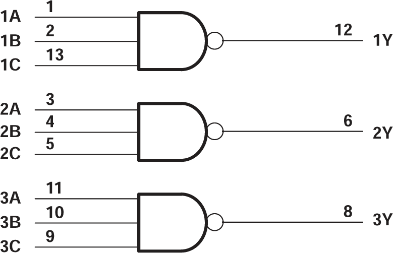
Functional Block Diagram

SN54ACT10 SN74ACT10 Logic Diagram, Each Gate
                                                  (Positive Logic) Figure 6-1 Logic Diagram, Each Gate (Positive Logic)

Pin numbers shown are for the D, DB, J, N, NS, PW, and W packages.