SCAS709C September   2003  – May 2024 SN74LVC257A-Q1

PRODUCTION DATA  

  1.   1
  2. Features
  3. Description
  4. Pin Configuration and Functions
  5. Specifications
    1. 4.1 Absolute Maximum Ratings
    2. 4.2 ESD Ratings
    3. 4.3 Recommended Operating Conditions
    4. 4.4 Thermal Information
    5. 4.5 Electrical Characteristics
    6. 4.6 Switching Characteristics
    7. 4.7 Operating Characteristics
  6. Parameter Measurement Information
  7. Detailed Description
    1. 6.1 Overview
    2. 6.2 Functional Block Diagram
    3. 6.3 Device Functional Modes
  8. Application and Implementation
    1. 7.1 Power Supply Recommendations
    2. 7.2 Layout
      1. 7.2.1 Layout Guidelines
      2. 7.2.2 Layout Example
  9. Device and Documentation Support
    1. 8.1 Documentation Support (Analog)
      1. 8.1.1 Related Links
    2. 8.2 Receiving Notification of Documentation Updates
    3. 8.3 Support Resources
    4. 8.4 Trademarks
    5. 8.5 Electrostatic Discharge Caution
    6. 8.6 Glossary
  10. Revision History
  11. 10Mechanical, Packaging, and Orderable Information

Description

The SN74LVC257A quadruple 2-line to 1-line data selector/multiplexer is designed for 2.7V to 3.6V VCC operation.

Package Information
PART NUMBER PACKAGE(1) PACKAGE SIZE(2) BODY SIZE(3)
SN74LVC257A-Q1 BQB (WQFN, 16) 3.5mm × 2.5mm 3.5mm × 2.5mm
D (SOIC, 16) 9.90 mm × 6mm 9.90 mm × 3.90 mm
PW (TSSOP, 16) 5.00 mm × 6.4mm 5.00 mm × 4.40 mm
The package size (length × width) is a nominal value and includes pins, where applicable.
The body size (length × width) is a nominal value and does not include pins.
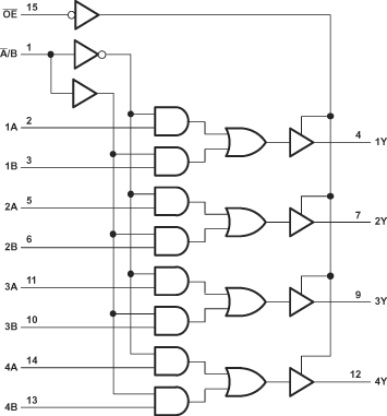
SN74LVC257A-Q1 Logic Diagram (Positive
                        Logic)Logic Diagram (Positive Logic)