SCAS915B June 2011 – July 2024 SN74AC14-Q1
PRODMIX
3 Pin Configuration and Functions
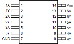
 Figure 3-1 PW Package, 14-Pin TSSOP (Top View)
 Figure 3-2 BQA Package, 14-Pin WQFN
(Top View)
Figure 3-2 BQA Package, 14-Pin WQFN
(Top View)| PIN | I/O | DESCRIPTION | |
|---|---|---|---|
| NAME | N.O. | ||
| 1A | 1 | Input | Channel 1, Input A |
| 1Y | 2 | Output | Channel 1, Output Y |
| 2A | 3 | Input | Channel 2, Input A |
| 2Y | 4 | Output | Channel 2, Output Y |
| 3A | 5 | Input | Channel 3, Input A |
| 3Y | 6 | Output | Channel 3, Output Y |
| GND | 7 | — | Ground |
| 4Y | 8 | Output | Channel 4, Output Y |
| 4A | 9 | Input | Channel 4, Input A |
| 5Y | 10 | Output | Channel 5, Output Y |
| 5A | 11 | Input | Channel 5, Input A |
| 6Y | 12 | Output | Channel 6, Output Y |
| 6A | 13 | Input | Channel 6, Input A |
| VCC | 14 | — | Positive Supply |
| NC | — | Not internally connected | |
| Thermal Pad(1) | — | The thermal pad can be connected to GND or left floating. Do not connect to any other signal or supply. | |
(1) BQA package only.