SCAS991 April 2024 SN54SC8T541-SEP
ADVANCE INFORMATION
- 1
- 1 Features
- 2 Applications
- 3 Description
- 4 Pin Configuration and Functions
- 5 Specifications
- 6 Parameter Measurement Information
- 7 Detailed Description
- 8 Application and Implementation
- 9 Device and Documentation Support
- 10Revision History
- 11Mechanical, Packaging, and Orderable Information
7.3.1 SCxT Enhanced Input Voltage
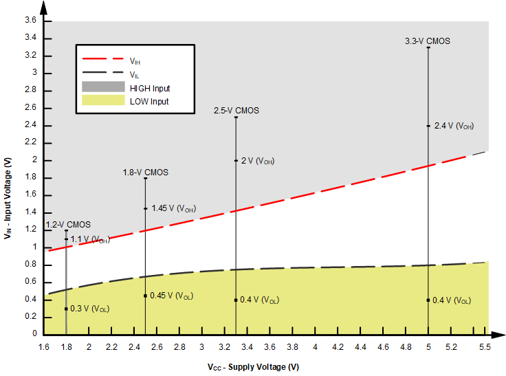
The SN54SC8T541-SEP belongs to TI's SCxT family of logic devices with integrated voltage level translation. This family of devices was designed with reduced input voltage thresholds to support up-translation, and inputs tolerant of signals with up to 5.5V levels to support down-translation. The output voltage will always be referenced to the supply voltage (VCC), as described in the Electrical Characteristics table. For proper functionality, input signals must remain at or below the specified VIH(MIN) level for a HIGH input state, and at or below the specified VIL(MAX) for a LOW input state. Figure 7-1 shows the typical VIH and VIL levels for the SCxT family of devices, as well as the voltage levels for standard CMOS devices for comparison.
The inputs are high impedance and are typically modeled as a resistor in parallel with the input capacitance given in the Electrical Characteristics. The worst case resistance is calculated with the maximum input voltage, given in the Absolute Maximum Ratings, and the maximum input leakage current, given in the Electrical Characteristics, using Ohm's law (R = V ÷ I).
The inputs require that input signals transition between valid logic states quickly, as defined by the input transition time or rate in the Recommended Operating Conditions table. Failing to meet this specification will result in excessive power consumption and could cause oscillations. More details can be found in the Implications of Slow or Floating CMOS Inputs application report.
Do not leave inputs floating at any time during operation. Unused inputs must be terminated at VCC or GND. If a system will not be actively driving an input at all times, a pull-up or pull-down resistor can be added to provide a valid input voltage during these times. The resistor value will depend on multiple factors; however, a 10-kΩ resistor is recommended and will typically meet all requirements.
 Figure 7-1 SCxT Input Voltage Levels