SCASE36 November 2024 SN74ACT595-Q1
PRODUCTION DATA
- 1
- 1 Features
- 2 Applications
- 3 Description
- 4 Pin Configuration and Functions
- 5 Specifications
- 6 Parameter Measurement Information
- 7 Detailed Description
- 8 Application and Implementation
- 9 Device and Documentation Support
- 10Revision History
- 11Mechanical, Packaging, and Orderable Information
3 Description
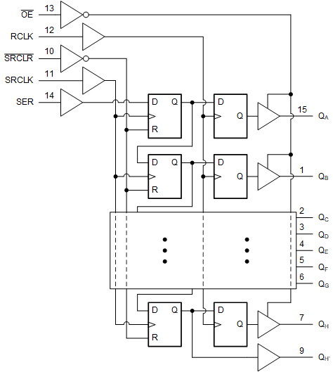
The SN74ACT595-Q1 device contains an 8-bit, serial-in, parallel-out shift register that feeds an 8-bit D-type storage register. The storage register has parallel outputs. Separate clocks are provided for both the shift and storage register. The shift register has a direct overriding clear (SRCLR) input, serial (SER) input, and a serial output (QH') for cascading. When the output-enable (OE) input is high, the register outputs are in a high-impedance state. Internal register data is not impacted by the operation of the OE input.
Device Information
| PART NUMBER | PACKAGE(1) | PACKAGE SIZE(2) | BODY SIZE(3) |
|---|---|---|---|
| SN74ACT595-Q1 | BQB (WQFN, 16) | 3.5mm × 2.5mm | 3.5mm × 2.5mm |
| PW (TSSOP , 16) | 5mm x 6.4mm | 5mm x 4.4mm |
(1) For more information, see
Section 11 .
(2) The package size (length ×
width) is a nominal value and includes pins, where applicable.
(3) The body size (length ×
width) is a nominal value and does not include pins.
 Functional Diagram