SCDA030 November 2020 MUX36S16 , TMUX1108 , TMUX1109 , TMUX1136 , TMUX1308 , TMUX6136
3 Multiplexer Specifications
-
Signal voltage range – Signal voltage ranges will vary depending on the output of the sensor and whether differential voltages with negative input swings or single-ended outputs are evident. Not all multiplexing devices can handle negative voltages, so finding a device that shows the signal switch input/output voltage whose lower limitations are below 0 V would be required for negative signal applications. This is often defined as either Vs, Vd, or Vi/o. Devices such as the TMUX6136 support a wide range of input signals ranging from –16.5 V to 16.5 V while still maintaining a low RON and CON.
-
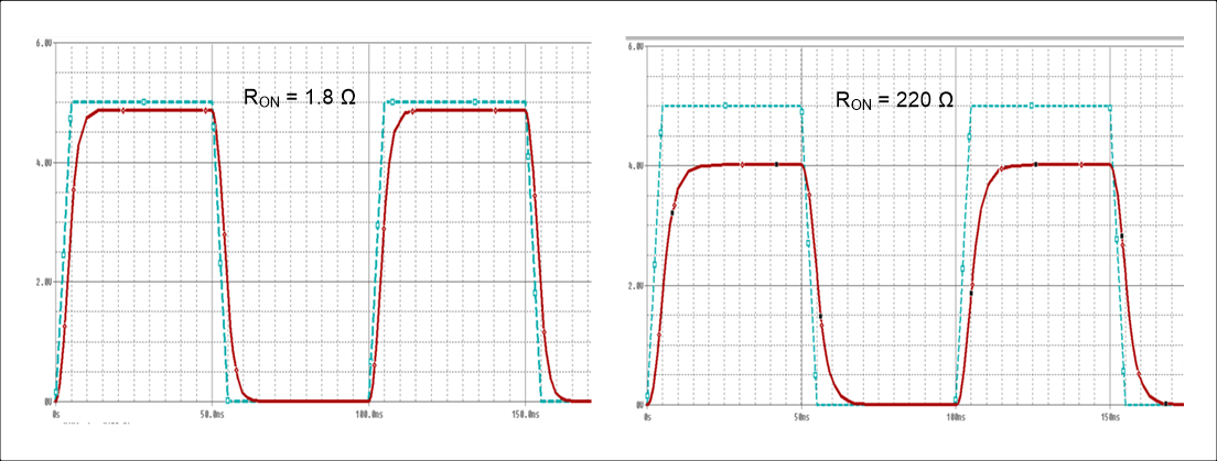
On-resistance (RON) – This is the resistance across the signal switch when the switch is turned on. A lower RON device, such as the TMUX1136, is especially useful in systems where the signal will not be amplified since the voltage will not drop across the signal switch and a close-to-original sensor input signal will be retained. If the design calls for an op amp or buffer in front of the built-in ADC of the MCU, a lower RON will decrease the gain error. Gain errors are heavily dependent on the load but minimizing the RON can still be beneficial. Furthermore, larger RON values create an offset voltage error when leakage current flows through the multiplexer. Simulations in Figure 3-1 illustrate the benefits of a low RON, modeling the TMUX1136 on the left. Here a 10-MHz signal is passed, with a 1-kΩ, 5-pF load. The 1.8-Ω RON of the TMUX1136 allows for proper signal pass-through and ensures that the signal integrity is maintained closely. An increase in the propogation delay due to a higher RC time constant is observed along with a decay in the overall signal.
Figure 3-1 illustrates that a lower on-resistance (TMUX1136 on left) enables lower distortion and errors in signal transmission.
 Figure 3-1 Comparison of
On-Resistance Impact on Signal.
 -
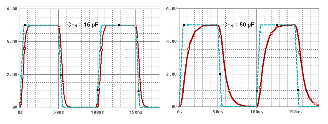
On-capacitance (CON) – This is the capacitance relative to ground seen by the system when the signal switch of the multiplexer is conducting. A low CON device, such as TMUX1308, allows for quicker response time, optimizing the sampling rate that can be achieved as well as widening the bandwidth. When using an op amp or buffer in front of the built-in ADC of the MCU, a lower CON will have less negative effects on stability. Figure 3-2 illustrates the effects of on-capacitance on digital signals. The 15-pF device on the left is a simulation of the TMUX1308 signal switch capabilities at 10 MHz. A lower on-capacitance will minimize the RC time constant, allowing for the signal to maintain its integrity. The benefits of a low CON is described more in more detail in the Improving Stability Issues with Low CON Multiplexers Application Note.
Figure 3-2 illustrates that a lower on-capacitance (TMUX1308 on left) provides less smoothing of the original (cyan) signal.
 Figure 3-2 Comparison of
On-Capacitance Impact on Signal.
 -
On-leakage current (IS(ON) / ID(ON)) – This is the leakage current measured across the signal switch while the switch is in the ON state. This should be a very small value as a high leakage current could corrupt data or load a bus that should be isolated. The voltage error associated with the leakage current is represented by the equation Verror = (RON + Rsource) × ION, where Rsource is the internal resistance of your voltage source. When switching between high-impedance sources such as accelerometers, optical and chemical sensors, the RON can be ignored in this equation, leaving the voltage error approximation to be ION × Rsource. When supplied with a 5-V supply, the TMUX1108 and TMUX1109 see typical RON and leakage current values of
2.5 Ω and 3 pA, respectively. This helps to reduce the voltage error and are great devices for use in high-precision applications.
-
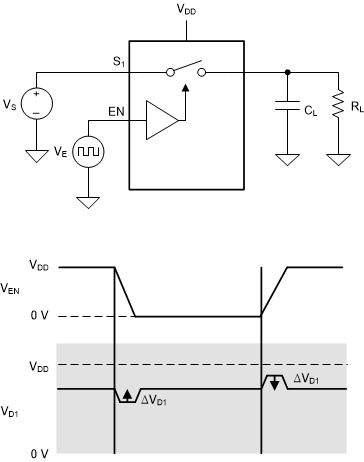
Charge injection (QC) – This is the measurement of unwanted coupling from the control pin into the signal switch. The charge induced by switching the inputs high or low will be seen on the signal switch. Charge injection is measured in Coulombs (C). While the charge injection occurs the signal on the data path will not be reliable, slowing down your sampling rate. This is illustrated for clearer understanding in Figure 3-3.
 Figure 3-3 Charge
Injection.