SCDS220L November 2006 – October 2024 TS3USB221
PRODUCTION DATA
- 1
- 1 Features
- 2 Applications
- 3 Description
- 4 Pin Configuration and Functions
-
5 Specifications
- 5.1 Absolute Maximum Ratings
- 5.2 ESD Ratings
- 5.3 Recommended Operating Conditions
- 5.4 Thermal Information
- 5.5 Electrical Characteristics
- 5.6 Dynamic Electrical Characteristics, VCC = 3.3V ± 10%
- 5.7 Dynamic Electrical Characteristics, VCC = 2.5V ± 10%
- 5.8 Switching Characteristics, VCC = 3.3V ± 10%
- 5.9 Switching Characteristics, VCC = 2.5V ± 10%
- 5.10 Typical Characteristics
- 6 Parameter Measurement Information
- 7 Detailed Description
- 8 Application and Implementation
- 9 Device and Documentation Support
- 10Revision History
- 11Mechanical, Packaging, and Orderable Information
3 Description
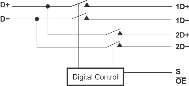
The TS3USB221 is a high-bandwidth switch specially designed for the switching of high-speed USB 2.0 signals in handset and consumer applications, such as cell phones, digital cameras, and notebooks with hubs or controllers with limited USB I/Os. The wide bandwidth (1.1GHz) of this switch allows signals to pass with minimum edge and phase distortion. The device multiplexes differential outputs from a USB host device to one of two corresponding outputs. The switch is bidirectional and offers little or no attenuation of the high-speed signals at the outputs. The TS3USB221 is designed for low bit-to-bit skew and high channel to channel noise isolation. The TS3USB221 is also compatible with various standards, such as high-speed USB 2.0 (480Mbps).
| PART NUMBER | PACKAGE(1) | PACKAGE SIZE(2) |
|---|---|---|
| TS3USB221 | DRC (VSON, 10) | 3mm × 3mm |
| RSE (UQFN, 10) | 2mm × 1.5mm |
 Block Diagram