SCDS220M November 2006 – November 2024 TS3USB221
PRODUCTION DATA
- 1
- 1 Features
- 2 Applications
- 3 Description
- 4 Pin Configuration and Functions
-
5 Specifications
- 5.1 Absolute Maximum Ratings
- 5.2 ESD Ratings
- 5.3 Recommended Operating Conditions
- 5.4 Thermal Information
- 5.5 Electrical Characteristics
- 5.6 Dynamic Electrical Characteristics, VCC = 3.3V ± 10%
- 5.7 Dynamic Electrical Characteristics, VCC = 2.5V ± 10%
- 5.8 Switching Characteristics, VCC = 3.3V ± 10%
- 5.9 Switching Characteristics, VCC = 2.5V ± 10%
- 5.10 Typical Characteristics
- 6 Parameter Measurement Information
- 7 Detailed Description
- 8 Application and Implementation
- 9 Device and Documentation Support
- 10Revision History
- 11Mechanical, Packaging, and Orderable Information
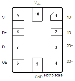
4 Pin Configuration and Functions
 Figure 4-1 DRC Package, 10-Pin VSON
(Top View)
 Figure 4-3 RSE Package, 10-Pin UQFB
(Bottom View)
 Figure 4-2 RSE Package, 10-Pin UQFN
(Top View)
Figure 4-2 RSE Package, 10-Pin UQFN
(Top View)Table 4-1 Pin Functions
| PIN | TYPE(1) | DESCRIPTION | |
|---|---|---|---|
| NAME | NO. | ||
| 1D+ | 1 | I/O | USB port 1 |
| 1D– | 2 | I/O | |
| 2D+ | 3 | I/O | USB port 2 |
| 2D– | 4 | I/O | |
| GND | 5 | — | Ground |
| OE | 6 | I | Bus-switch enable |
| D– | 7 | I/O | Common USB port |
| D+ | 8 | I/O | |
| S | 9 | I | Select input |
| VCC | 10 | — | Supply voltage |
(1) I = input, O = output