SCDS343F May   2013  – August 2018 TS3DV642

PRODUCTION DATA.  

  1. Features
  2. Applications
  3. Description
    1.     Device Images
      1.      Simplified Schematic
  4. Revision History
  5. Pin Configuration and Functions
    1.     Pin Functions
  6. Specifications
    1. 6.1 Absolute Maximum Ratings
    2. 6.2 ESD Ratings
    3. 6.3 Recommended Operating Conditions
    4. 6.4 Thermal Information
    5. 6.5 Electrical Characteristics
    6. 6.6 Dynamic Characteristics
    7. 6.7 Switching Characteristics
    8. 6.8 Typical Characteristics
  7. Parameter Measurement Information
  8. Detailed Description
    1. 8.1 Overview
    2. 8.2 Functional Block Diagram
    3. 8.3 Feature Description
    4. 8.4 Device Functional Modes
  9. Application and Implementation
    1. 9.1 Application Information
    2. 9.2 Typical Application
      1. 9.2.1 Display Port (DP) Application
        1. 9.2.1.1 Design Requirements
        2. 9.2.1.2 Detailed Design Procedure
        3. 9.2.1.3 Application Curves
      2. 9.2.2 Docking Application
        1. 9.2.2.1 Design Requirements
        2. 9.2.2.2 Detailed Design Procedure
        3. 9.2.2.3 Application Curves
      3. 9.2.3 HDMI Application
        1. 9.2.3.1 Design Requirements
        2. 9.2.3.2 Detailed Design Procedure
        3. 9.2.3.3 Application Curves
  10. 10Power Supply Recommendations
  11. 11Layout
    1. 11.1 Layout Guidelines
    2. 11.2 Layout Example
  12. 12Device and Documentation Support
    1. 12.1 Receiving Notification of Documentation Updates
    2. 12.2 Community Resources
    3. 12.3 Trademarks
    4. 12.4 Electrostatic Discharge Caution
    5. 12.5 Glossary
  13. 13Mechanical, Packaging, and Orderable Information

Device Functional Modes

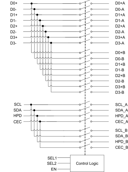
TS3DV642 logic_cds343.gifFigure 20. Logic Diagram

Table 1 lists the device functions for the TS3DV642 device.

Table 1. Functional Table

EN SEL1 SEL2 FUNCTION
L X X Switch disabled. All channels are Hi-Z.
H L L Channel D0+/D0– to D0+A/D0–A is ON. All the other channels (D1+/D1-, D2+/D2-, D3+/D3-, SCL, SDA, HPD, CEC) are Hi-Z.
H L H Channel D0+/D0– to D0+B/D0–B is ON. All the other channels (D1+/D1-, D2+/D2-, D3+/D3-, SCL, SDA, HPD, CEC) are Hi-Z.
H H L All A channels are enabled. All B channels are Hi-Z.
H H H All B channels are enabled. All A channels are Hi-Z.