SCDS420E September 2020 – July 2024 TMUX6219
PRODUCTION DATA
- 1
- 1 Features
- 2 Applications
- 3 Description
- 4 Pin Configuration and Functions
-
5 Specifications
- 5.1 Absolute Maximum Ratings
- 5.2 ESD Ratings
- 5.3 Thermal Information
- 5.4 Recommended Operating Conditions
- 5.5 Source or Drain Continuous Current
- 5.6 ±15 V Dual Supply: Electrical Characteristics
- 5.7 ±15 V Dual Supply: Switching Characteristics
- 5.8 36 V Single Supply: Electrical Characteristics
- 5.9 36 V Single Supply: Switching Characteristics
- 5.10 12 V Single Supply: Electrical Characteristics
- 5.11 12 V Single Supply: Switching Characteristics
- 5.12 +5 V / -8 V Dual Supply: Electrical Characteristics
- 5.13 +5 V / -8 V Dual Supply: Switching Characteristics
- 5.14 ±5 V Dual Supply: Electrical Characteristics
- 5.15 ±5 V Dual Supply: Switching Characteristics
- 5.16 Typical Characteristics
-
6 Parameter Measurement Information
- 6.1 On-Resistance
- 6.2 Off-Leakage Current
- 6.3 On-Leakage Current
- 6.4 Transition Time
- 6.5 tON(EN) and tOFF(EN)
- 6.6 Break-Before-Make
- 6.7 tON (VDD) Time
- 6.8 Propagation Delay
- 6.9 Charge Injection
- 6.10 Off Isolation
- 6.11 Crosstalk
- 6.12 Bandwidth
- 6.13 THD + Noise
- 6.14 Power Supply Rejection Ratio (PSRR)
- 7 Detailed Description
- 8 Application and Implementation
- 9 Power Supply Recommendations
- 10Layout
- 11Device and Documentation Support
- 12Revision History
- 13Mechanical, Packaging, and Orderable Information
3 Description
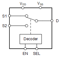
The TMUX6219 is a complementary metal-oxide semiconductor (CMOS) switch in a single channel, 2:1 (SPDT) configuration. The device works with single supply (4.5V to 36V), dual supplies (±4.5V to ±18V), or asymmetric supplies (such as VDD = 5V, VSS = −8V). The TMUX6219 supports bidirectional analog and digital signals on the source (Sx) and drain (D) pins ranging from VSS to VDD.
The TMUX6219 can be enabled or disabled by controlling the EN pin. When disabled, both signal path switches are off. When enabled, the SEL pin can be used to turn on signal path 1 (S1 to D) or signal path 2 (S2 to D). All logic control inputs support logic levels from 1.8V to VDD, ensuring both TTL and CMOS logic compatibility when operating in the valid supply voltage range. Fail-Safe Logic circuitry allows voltages on the control pins to be applied before the supply pin, protecting the device from potential damage.
The TMUX6219 is part of the precision switches and multiplexers family of devices. These devices have very low on and off leakage currents and low charge injection, allowing them to be used in high precision measurement applications.
| PART NUMBER | PACKAGE(1) | PACKAGE SIZE (2) |
|---|---|---|
| TMUX6219 | DGK (VSSOP, 8) | 3mm × 4.9mm |
| RQX (WSON, 8) | 2mm × 3mm |
 TMUX6219 Block Diagram