SCDS429G February 2021 – July 2024 TMUX7234
PRODUCTION DATA
- 1
- 1 Features
- 2 Applications
- 3 Description
- 4 Pin Configuration and Functions
-
5 Specifications
- 5.1 Absolute Maximum Ratings
- 5.2 ESD Ratings
- 5.3 Thermal Information
- 5.4 Recommended Operating Conditions
- 5.5 Source or Drain Continuous Current
- 5.6 ±15 V Dual Supply: Electrical Characteristics
- 5.7 ±15 V Dual Supply: Switching Characteristics
- 5.8 ±20 V Dual Supply: Electrical Characteristics
- 5.9 ±20 V Dual Supply: Switching Characteristics
- 5.10 44 V Single Supply: Electrical Characteristics
- 5.11 44 V Single Supply: Switching Characteristics
- 5.12 12 V Single Supply: Electrical Characteristics
- 5.13 12 V Single Supply: Switching Characteristics
- 5.14 Typical Characteristics
-
6 Parameter Measurement Information
- 6.1 On-Resistance
- 6.2 Off-Leakage Current
- 6.3 On-Leakage Current
- 6.4 Transition Time
- 6.5 tON(EN) and tOFF(EN)
- 6.6 Break-Before-Make
- 6.7 tON (VDD) Time
- 6.8 Propagation Delay
- 6.9 Charge Injection
- 6.10 Off Isolation
- 6.11 Crosstalk
- 6.12 Bandwidth
- 6.13 THD + Noise
- 6.14 Power Supply Rejection Ratio (PSRR)
- 7 Detailed Description
- 8 Application and Implementation
- 9 Power Supply Recommendations
- 10Layout
- 11Device and Documentation Support
- 12Revision History
- 13Mechanical, Packaging, and Orderable Information
7.3.6 Ultra-Low Charge Injection
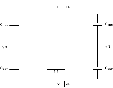
The TMUX7234 has a transmission gate topology, as shown in Figure 7-1. Any mismatch in the stray capacitance associated with the NMOS and PMOS causes an output level change whenever the switch is opened or closed.
 Figure 7-1 Transmission Gate Topology
The TMUX7234 contains specialized architecture to reduce charge injection on the source (Sx). To further reduce charge injection in a sensitive application, a compensation capacitor (Cp) can be added on the drain (D). This will ensure that excess charge from the switch transition will be pushed into the compensation capacitor on the drain (D) instead of the source (Sx). As a general rule of thumb, Cp should be 20x larger than the equivalent load capacitance on the source (Sx). Figure 7-2 shows charge injection variation with different compensation capacitors on the drain side. This plot was captured on the TMUX7219 as part of the TMUX72xx family with a 100pF load capacitance.
 Figure 7-2 Charge Injection Compensation