SCDS480 September 2024 TMUX1219-Q1
PRODUCTION DATA
- 1
- 1 Features
- 2 Applications
- 3 Description
- 4 Pin Configuration and Functions
-
5 Specifications
- 5.1 Absolute Maximum Ratings
- 5.2 ESD Ratings
- 5.3 Recommended Operating Conditions
- 5.4 Thermal Information
- 5.5 Electrical Characteristics (VDD = 5V ±10 %)
- 5.6 Electrical Characteristics (VDD = 3.3V ±10 %)
- 5.7 Electrical Characteristics (VDD = 1.8V ±10 %)
- 5.8 Electrical Characteristics (VDD = 1.2V ±10 %)
- 5.9 Typical Characteristics
- 6 Parameter Measurement Information
- 7 Detailed Description
- 8 Application and Implementation
- 9 Power Supply Recommendations
- 10Layout
- 11Device and Documentation Support
- 12Revision History
- 13Mechanical, Packaging, and Orderable Information
3 Description
The TMUX1219-Q1 is a general purpose complementary metal-oxide semiconductor (CMOS) single-pole double-throw (SPDT) switch. The TMUX1219-Q1 switches between two source inputs based on the state of the SEL pin. Wide operating supply of 1.08V to 5.5V allows for use in a wide array of automotive applications. The device supports bidirectional analog and digital signals on the source (Sx) and drain (D) pins ranging from GND to VDD. A low supply current of 4nA enables use in portable applications.
All logic inputs have 1.8V logic compatible thresholds, ensuring both TTL and CMOS logic compatibility when operating in the valid supply voltage range. Fail-Safe Logic circuitry allows voltages on the control pins to be applied before the supply pin, protecting the device from potential damage.
| PART NUMBER | PACKAGE(1) | BODY SIZE (NOM) |
|---|---|---|
| TMUX1219-Q1 | SOT-23 (6) | 2.90mm x 1.60mm |
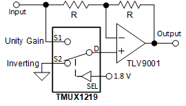
 Application Example
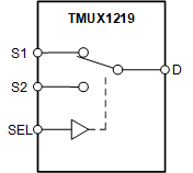
 Block Diagram