SCDU038 April 2024 TMUX6221 , TMUX7221
2.2 Setup
- The default setup of the board has all 10 generic pathways grounded, with the IC set to single supply operation as the pad voltage is also set to ground.
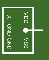
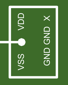
- All 10 generic signal pathway headers contain six pins. Figure 2-1 and Figure 2-2 show the generalized pinout of the headers for the left and right side of the board respectively. Note that the orientation is based on J11 being on the top of the board.
-
 Figure 2-1 Left Side Jumper
(J1-J5) Configuration or Pinout
 Figure 2-2 Right Side Jumper
(J6-J10) Configuration or Pinout