SCEA121 june 2023 LMH5485-SEP
Design Goals
| Parameter | Design Requirement |
|---|---|
| FDA Input Type | Single-ended |
| Input AC Supply Voltage | AC Coupled 2-MHz, 2-Vpp Sine Wave |
| Component Rating | Space |
| FDA Output, ADC Input | 3.2 Vpp |
| FDA Output Common Mode | 0.95 V |
| Filter | Third-order passive Butterworth low-pass filter with 4-MHz cutoff |
| Termination Resistor | No termination resistor |
| LMH5485-SEP Radiation Capability | Radiation tolerant up to 30-krad (Si) total ionizing dose (TID) |
Design Description
This space-grade circuit design shows a single-ended-to-differential (SE-to-Diff) ADC driver utilizing the LMH5485-SEP and an analog-to-digital converter (ADC) with a common mode of 0.95 V and an input range of 3.2 Vpp. The LMH5485-SEP is a space-grade, low-power, high-speed fully-differential amplifier that is mainly used to drive high-performance ADCs. High-performance ADCs are low-noise, ultra-low power, high-speed, dual-channel devices that are used in many space applications. Some of these include: imaging, spectroscopy, radar, control loops, instrumentation, and so forth. Since the ADC accepts a differential signal, fully-differential amplifiers (FDA) are a good choice for designing a circuit compared to using two op amps. Aside from providing a balanced output signal, FDAs have other great benefits. Some of these benefits include:
|
|
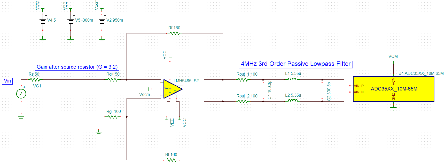
The following image shows the completed circuit design.
 Completed Single-Ended-to-Differential ADC Driver Circuit
The circuit illustrated in the previous image starts with a single-ended AC source with a 50-Ω source resistance. This source is provided to the LMH5485 fully-operational amplifier. With the feedback resistor values, the gain of the amplifier is 3.2. The output of the FDA then enters a third-order passive Butterworth low-pass filter with a cutoff frequency of 4 MHz before going to the input of the ADC.
Design Steps
- Two sources are required to power the FDA, VCC, and VEE. VCC is set to 5 V and VEE is set to –300 mV. This FDA requires a headroom of 0.2 V–0.3 V at the input rails, which is the reason for –300 mV on VEE.
- Determine the source resistance, gain, and input signal for the amplifier. For this design the desired source resistance is 50 Ω, gain is 3.2 and the input signal is 2 Vpp. The simulation found that the 50-Ω source resistor divided the input voltage by half when the termination resistor was not present; therefore, the supply voltage is 2 Vpp. In actuality, the voltage is 1 Vpp after the 50-Ω source resistance. To have an impedance matched circuit, Rg1 can match the source resistor, therefore, Rg1 is 50 Ω.
- Calculating Rg2 uses the next
three equations:
Since a termination resistor (Rt) is not used, treat Rt as infinity; therefore, 1/Rt cancels out.
As the equation demonstrates, Rg2 is always twice the resistor value of Rg1.
- From the calculated values, the
value of the feedback resistor (Rf) can be determined.
As seen in design step 4, since a termination resistor (Rt) is not being used, the bottom part of the fraction equals to 1. This equation can be rearranged to solve for Rf. The updated equation follows:
- After designing the FDA stage,
create a third-order passive Butterworth low-pass filter (LPF). The cutoff
frequency is 2 MHz; however, the LPF was calculated at 4 MHz to make sure that a
2-MHz signal remains above –3 dB. The following equation was used to calculate
the component values for the LPF:
After putting all the components together, 4-MHz 3rd Order Passive Butterworth Low-Pass Filter shows the completed filter. Since this design is differential, the resistors and inductors can be present on both output rails. Therefore, the value of the resistor and inductor is divided by half for each output rail. The input resistors of the filter are 100 Ω. The output resistor named “ADC Load” is a dummy load that represents the internal ADC load which is not part of the filter.
 4-MHz 3rd-Order Passive Butterworth
Low-Pass Filter
Design Simulations
VIN and VOUT Waveforms
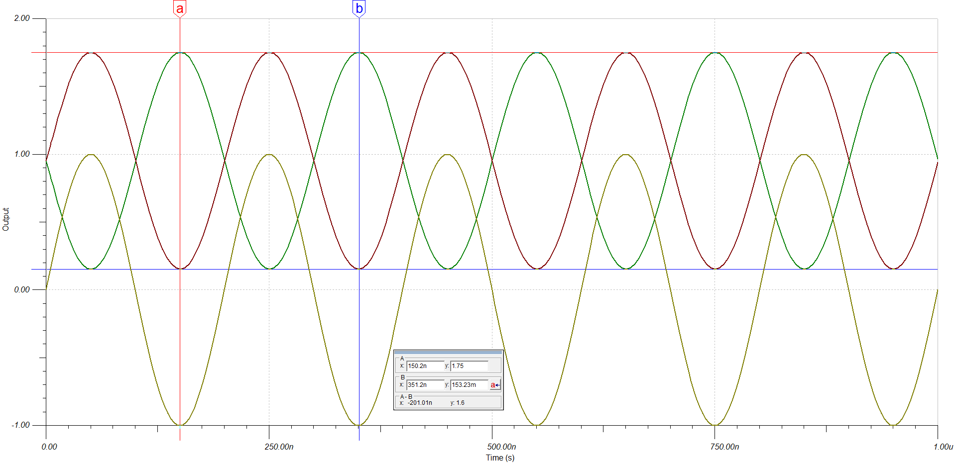
Single-Ended VIN vs Differential VOUT Waveforms shows the input and output of the FDA. Yellow is the input source, red is the positive output, and green is the negative output. The input is 2 Vpp (1 Vpp after the source resistor) and the positive and negative output swing is 1.6 Vpp. Combining the two differential signals, positive and negative, makes the output swing 3.2 Vpp. Note that the output has a common-mode voltage of 0.95 V.
 Single-Ended VIN vs Differential VOUT Waveforms
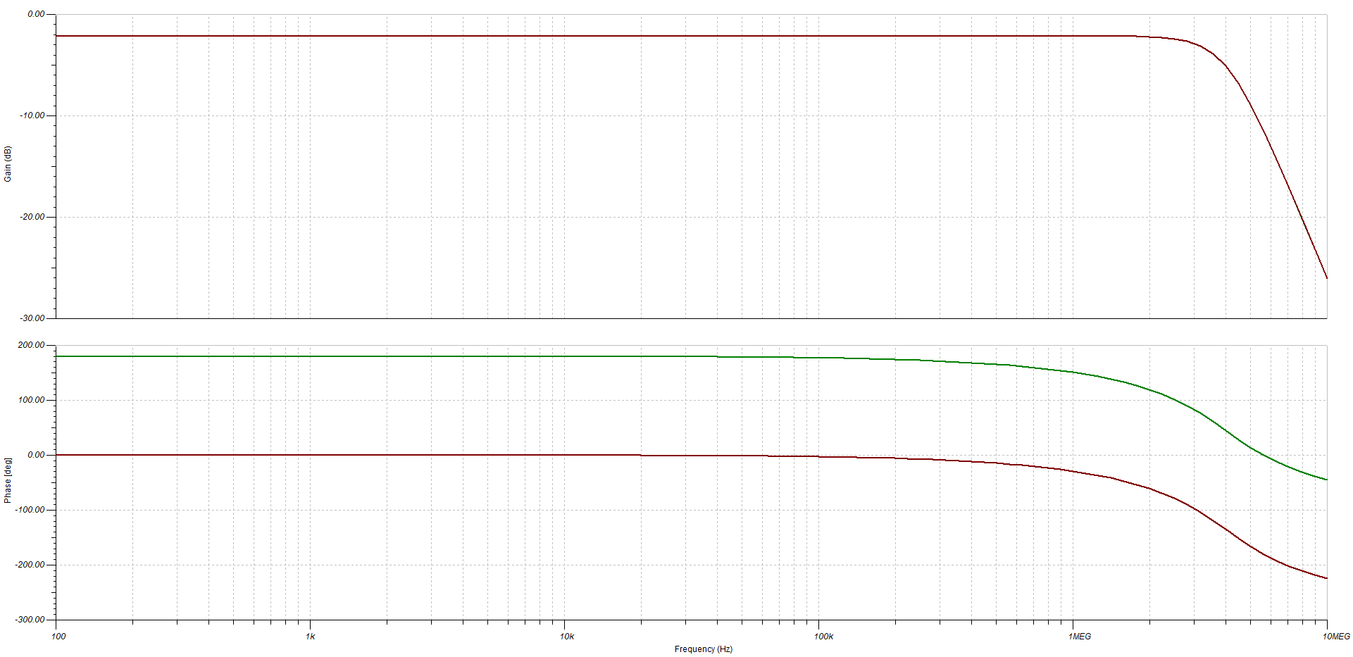
Gain and Phase Bode Plots shows the gain and phase plots of the second-order passive low-pass filter. As the following plot shows, the cutoff frequency is at 4 MHz. This is made to keep the actual cutoff frequency of 2 MHz above –3-dB gain.
 Gain and Phase Bode Plots
Stability
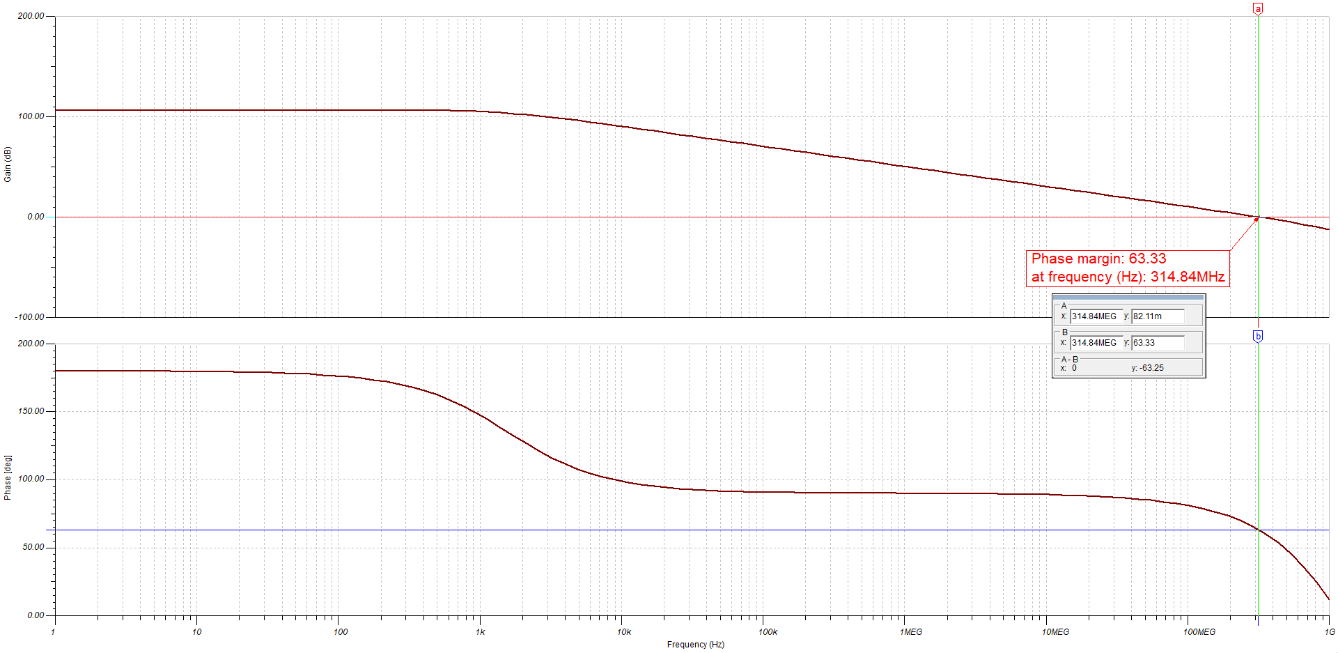
Phase margin of an amplifier is the amount of phase shift when the gain of an amplifier is above 0 dB. An amplifier is considered not stable once the open loop gain falls below 0 dB or when the phase margin drops below 60 degrees. In this case, the open loop gain drops below 0 after 314.84 MHz, with a phase margin of 63.33 degrees as Stability Gain and Phase Bode Plots shows. This is more than enough for the application since the amplifier is only operating at 2 MHz.
 Stability Gain and Phase Bode Plots
Implementing an FDA is a very efficient way to power an ADC. The reduced number of components and increased resistance to external noise and even-order harmonics are some of the great benefits that the FDA offers. The FDA can be intimidating at a first glance, however, when looking into the design steps, the process is very user friendly. In this design, the FDA outputs a desired 3.2 Vpp output with a common mode of 0.95 V. The low-pass filter after the FDA has a cutoff frequency of 4 MHz and since it is a 3rd-order filter, the cutoff is very sharp which removes any unwanted harmonics of the passing frequency.
Additional Resources
- Texas Instruments, LMH5485-SEP Radiation tolerant, space-enhanced plastic, 850-MHz fully differential amplifier product page
- Texas Instruments, LMH5485-SEP Radiation Tolerant Negative Rail Input, Rail-to-Rail Output, Precision, 850-MHz Fully Differential Amplifier data sheet
- Texas Instruments, Input impedance matching with fully differential amplifiers analog design journal
- Texas Instruments, Fully differential amplifier design in high-speed data acquisition systems analog design journal
- Texas Instruments, Fully-Differential Amplifiers application note