SCES481E August 2003 – August 2024 SN74LVC74A-Q1
PRODUCTION DATA
3 Pin Configuration and Functions
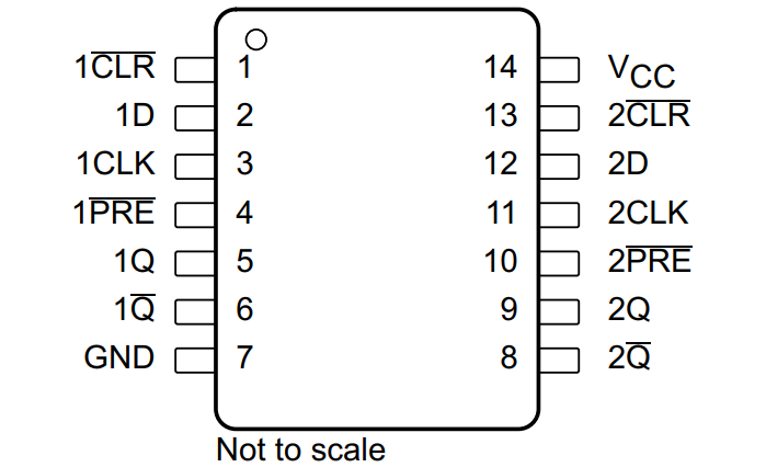
 Figure 3-1 D or PW Package, 14-Pin SOIC or TSSOP(Top View)
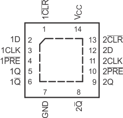
 Figure 3-2 BQA Package14-Pin WQFN With Exposed Thermal Pad(Top View)
Table 3-1 Pin Functions
| PIN | I/O(1) | DESCRIPTION | |
|---|---|---|---|
| NAME | SOIC, TSSOP, VQFN | ||
| 1CLK | 3 | I | Channel 1 clock input |
| 1 CLR | 1 | I | Channel 1 clear input. Pull low to set Q output low. |
| 1D | 2 | I | Channel 1 data input |
| 1 PRE | 4 | I | Channel 1 preset input. Pull low to set Q output high. |
| 1Q | 5 | O | Channel 1 output |
| 1 Q | 6 | O | Channel 1 inverted output |
| 2CLK | 11 | I | Channel 2 clock input |
| 2 CLR | 13 | I | Channel 2 clear input. Pull low to set Q output low. |
| 2D | 12 | I | Channel 2 data input |
| 2 PRE | 10 | I | Channel 2 preset input. Pull low to set Q output high. |
| 2Q | 9 | O | Channel 2 output |
| 2 Q | 8 | O | Channel 2 Inverted output |
| GND | 7 | — | Ground |
| NC | — | — | No connect |
| VCC | 14 | — | Supply |
| Thermal pad | — | Connect the GND pin to the exposed thermal pad for correct operation. Connect the thermal pad to any internal PCB ground plane using multiple vias for good thermal performance. | |
(1) I = input, O = output, P = power,
FB = feedback, GND = ground, N/A = not applicable