SCES677F September 2006 – June 2024 SN74LVC1T45-Q1
PRODUCTION DATA
- 1
- 1Features
- 2Applications
- 3Description
- 4Pin Configuration and Functions
-
5Specifications
- 5.1 Absolute Maximum Ratings
- 5.2 ESD Ratings
- 5.3 Recommended Operating Conditions
- 5.4 Thermal Information
- 5.5 Electrical Characteristics
- 5.6 Switching Characteristics: VCCA = 1.8V ±0.15V
- 5.7 Switching Characteristics: VCCA = 2.5V ±0.2V
- 5.8 Switching Characteristics: VCCA = 3.3V ±0.3V
- 5.9 Switching Characteristics: VCCA = 5V ±0.5V
- 5.10 Typical Characteristics
- Parameter Measurement Information
- 6Detailed Description
- Application and Implementation
- 7Device and Documentation Support
- 8Revision History
- 9Mechanical, Packaging, and Orderable Information
3 Description
The SN74LVC1T45-Q1 device is a single-bit, noninverting bus transceiver that uses two separate configurable power supply rails. The A-port is designed to track VCCA. VCCA accepts any supply voltage from 1.65V to 5.5V. The B-port is designed to track VCCB. VCCB accepts any supply voltage from 1.65V to 5.5V. This allows for universal low-voltage bidirectional translation between any of the 1.8V, 2.5V, 3.3V, and 5V voltage nodes.
The SN74LVC1T45-Q1 device is a single-bit, non-inverting level translator. The fully configurable dual-rail design allows each port to overate over the full 1.65V to 5.5V power supply range. This device is an excellent choice for applications that need a wide bidirectional translation range.
The SN74LVC1T45-Q1 is designed so that the DIR input is powered by VCCA.
This device is fully specified for partial-power-down applications using Ioff. The Ioff circuitry disables the outputs, preventing damaging current backflow through the device when it is powered down.
The VCC isolation feature is designed so that if either VCC input is at GND, then both ports are in the high-impedance state.
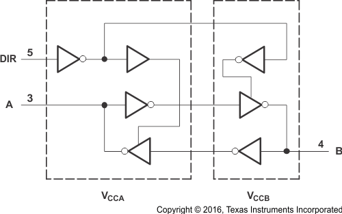
 Logic Diagram (Positive Logic)