SCES861F June 2015 – November 2024 TXS0108E-Q1
PRODUCTION DATA
- 1
- 1 Features
- 2 Applications
- 3 Description
- 4 Pin Configuration and Functions
-
5 Specifications
- 5.1 Absolute Maximum Ratings
- 5.2 ESD Ratings
- 5.3 Recommended Operating Conditions
- 5.4 Thermal Information
- 5.5 Electrical Characteristics: TA = –40°C to 125°C
- 5.6 Timing Requirements: VCCA = 1.5V ± 0.1 V
- 5.7 Timing Requirements: VCCA = 1.8V ± 0.15V
- 5.8 Timing Requirements: VCCA = 2.5V ± 0.2V
- 5.9 Timing Requirements: VCCA = 3.3V ± 0.3V
- 5.10 Switching Characteristics: VCCA = 1.5V ± 0.1V
- 5.11 Switching Characteristics: VCCA = 1.8V ± 0.15V
- 5.12 Switching Characteristics: VCCA = 2.5V ± 0.2V
- 5.13 Switching Characteristics: VCCA = 3.3V ± 0.3V
- 5.14 Typical Characteristics
- 6 Parameter Measurement Information
- 7 Detailed Description
- 8 Application and Implementation
- 9 Device and Documentation Support
- 10Revision History
- 11Mechanical, Packaging, and Orderable Information
6.1 Load Circuits
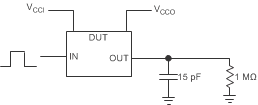
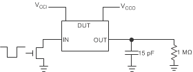
Figure 6-1 shows the push-pull driver circuit used for measuring data rate, pulse duration, propagation delay, output rise-time and fall-time. Figure 6-2 shows the open-drain driver circuit used for measuring data rate, pulse duration, propagation delay, output rise-time and fall-time.

A. VCCI is the VCC associated with the input port.
B. VCCO is the VCC associated with the output port.
Figure 6-1 Data Rate, Pulse Duration, Propagation Delay, Output Rise-Time And Fall-Time Measurement Using a Push-Pull Driver
A. VCCI is the VCC associated with the input port.
B. VCCO is the VCC associated with the output port.
Figure 6-2 Data Rate (10pF), Pulse Duration (10pF), Propagation Delay, Output Rise-Time And Fall-Time Measurement Using an Open-Drain Driver
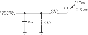
| TEST | S1 |
|---|---|
| tPZL,
tPLZ
(tdis) |
2 × VCCO |
| tPHZ, tPZH
(ten) |
Open |
A. tPLZ and tPHZ are the same as tdis.
B. tPZL and tPZH are the same as ten.
Figure 6-3 Load Circuit for Enable-Time and Disable-Time Measurement