SCES968 June 2024 TXS0104V-Q1
PRODUCTION DATA
- 1
- 1 Features
- 2 Applications
- 3 Description
- 4 Pin Configuration and Functions
-
5 Specifications
- 5.1 Absolute Maximum Ratings
- 5.2 ESD Ratings
- 5.3 Recommended Operating Conditions
- 5.4 Thermal Information (PW, BQA, RUT)
- 5.5 Electrical Characteristics
- 5.6 Switching Characteristics, VCCA = 1.8 ± 0.15V
- 5.7 Switching Characteristics, VCCA = 2.5 ± 0.2V
- 5.8 Switching Characteristics, VCCA = 3.3 ± 0.3V
- 5.9 Switching Characteristics: Tsk, TMAX
- 5.10 Typical Characteristics
- 6 Parameter Measurement Information
- 7 Detailed Description
- 8 Application and Implementation
- 9 Device and Documentation Support
- 10Revision History
- 11Mechanical, Packaging, and Orderable Information
6.1 Load Circuits
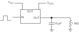
 Figure 6-1 Data Rate, Pulse Duration, Propagation Delay, Output Rise-Time and Fall-Time Measurement Using a Push-Pull Driver
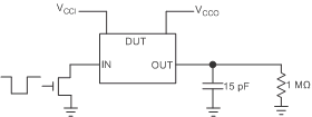
 Figure 6-2 Data Rate, Pulse Duration, Propagation Delay, Output Rise-Time and Fall-Time Measurement Using an Open-Drain Driver
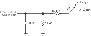
| TEST | S1 | ||
| tPZL / tPLZ (tdis) | 2 × VCCO | ||
| tPHZ / tPZH (ten) | Open | ||
- tPLZ and tPHZ are the same as tdis.
- tPZL and tPZH are the same as ten.
- VCCI is the VCC associated with the input port.
- VCCO is the VCC associated with the output port.