SCES968 June 2024 TXS0104V-Q1
PRODUCTION DATA
- 1
- 1 Features
- 2 Applications
- 3 Description
- 4 Pin Configuration and Functions
-
5 Specifications
- 5.1 Absolute Maximum Ratings
- 5.2 ESD Ratings
- 5.3 Recommended Operating Conditions
- 5.4 Thermal Information (PW, BQA, RUT)
- 5.5 Electrical Characteristics
- 5.6 Switching Characteristics, VCCA = 1.8 ± 0.15V
- 5.7 Switching Characteristics, VCCA = 2.5 ± 0.2V
- 5.8 Switching Characteristics, VCCA = 3.3 ± 0.3V
- 5.9 Switching Characteristics: Tsk, TMAX
- 5.10 Typical Characteristics
- 6 Parameter Measurement Information
- 7 Detailed Description
- 8 Application and Implementation
- 9 Device and Documentation Support
- 10Revision History
- 11Mechanical, Packaging, and Orderable Information
3 Description
This 4-bit non-inverting translator uses two separate configurable power-supply rails. The A port is designed to track VCCA. VCCA accepts any supply voltage from 1.65V to 3.6V. VCCA must be less than or equal to VCCB. The B port is designed to track VCCB. VCCB accepts any supply voltage from 2.3V to 5.5V. This allows for low-voltage bidirectional translation between any of the 1.8V, 2.5V, 3.3V, and 5V voltage nodes.
When the output-enable (OE) input is low, all outputs are placed in the high-impedance state.
The TXS0104V-Q1 is designed so that the OE input circuit is supplied by VCCA.
For the high-impedance state during power up or power down, tie OE to GND through a pull-down resistor; the current-sourcing capability of the driver determines the minimum value of the resistor.
| PART NUMBER | PACKAGE(1) | PACKAGE SIZE(2) |
|---|---|---|
| TXS0104V-Q1 | PW (TSSOP, 14) | 5mm × 6.4mm |
| BQA (WQFN, 12) | 3mm × 2.5mm | |
| RUT (UQFN, 12) | 2mm × 1.7mm |
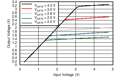
 Transfer Characteristics of an N-Channel Transistor