SCEU024 January 2022
2.2 Hardware Setup
This section will cover the six steps to take when evaluating a leaded Logic device using this EVM.
- Identify the package you will be using for the device being evaluated. As stated previously, this EVM has seven sections each of which supporting a non-leaded footprint. Break off the selected section (optional).
- Solder down the device. Since this EVM supports
small, non-leaded packages, this will likely require a hot air rework station.
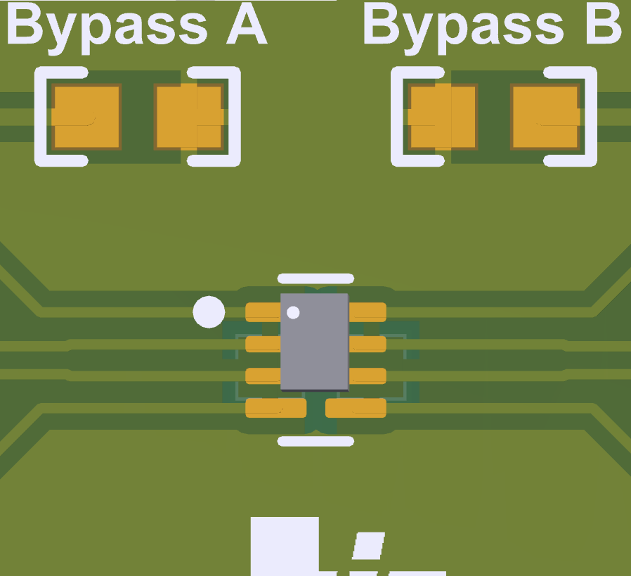
Figure 2-2 illustrates an example of proper placement of a DRY device on the footprint
that also supports the DTT package.
 Figure 2-2 6-pin DRY
Placement
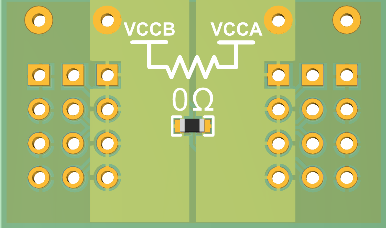
 - Ensure EVM is configured accordingly for dual
supply or single supply device. EVM comes default configured for dual supply
devices, but is easily configured using a 0-Ω resistor for single supply
devices. Figure 2-3 illustrates
how this is done.
 Figure 2-3 Single Supply
Configuration
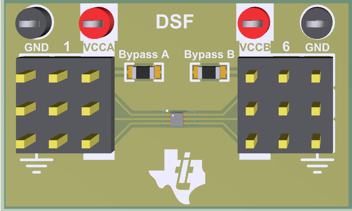
 - Interface with device pins. The kit includes twelve
4-pin headers and four supply test points. The headers can be cut to accomodate
the 5-pin and 6-pin footprints. An example of this, with the addition of bypass
capacitors for the supplies, can be seen in Figure 2-4. Note: The DPW section has the middle pad grounded to accommodate the
pin-3 GND of DPW devices.
 Figure 2-4 Fully Populated
Section
 - Before applying power to the EVM, ensure the proper supply configuration is in place to avoid shorting two supplies together.