SCHS051J November 1998 – August 2024 CD4066B , CD4066B-MIL
PRODUCTION DATA
6 Parameter Measurement Information
 Figure 6-1 Determination of ron as a Test Condition for Control-Input
High-Voltage (VIHC) Specification
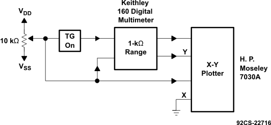 Figure 6-2 Channel On-State Resistance Measurement Circuit
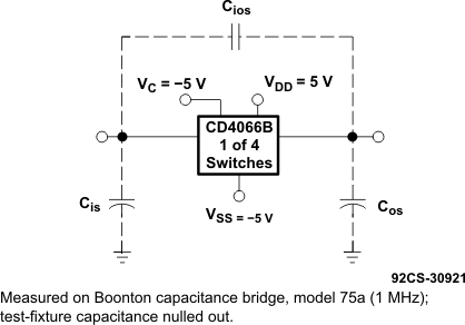 Figure 6-3 Typical On Characteristics for One of Four Channels
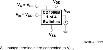 Figure 6-4 Off-Switch Input or Output Leakage
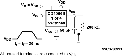 Figure 6-5 Propagation Delay Time Signal Input (Vis) to Signal Output
(Vos)
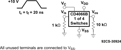 Figure 6-6 Crosstalk-Control Input to Signal Output
All unused
pins are connected to VSS.
Delay is
measured at Vos level of +10% from ground (turn-on) or on-state
output level (turn-off).
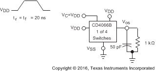
Figure 6-7 Propagation Delay, tPLH, tPHL Control-Signal
Output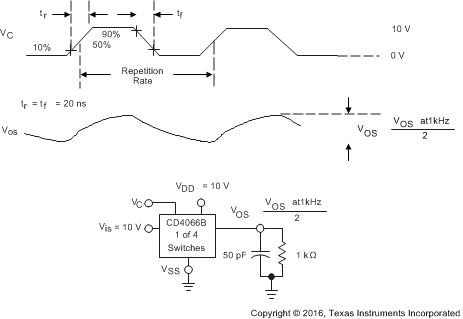
All unused
pins are connected to VSS.
Figure 6-8 Maximum Allowable Control-Input Repetition Rate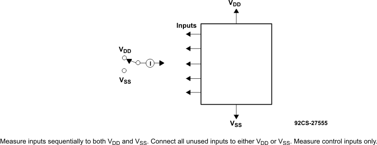 Figure 6-9 Input
Leakage-Current Test Circuit
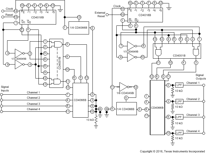 Figure 6-10 Four-Channel PAM Multiplex System Diagram