SCHS231E November 1998 – August 2024 CD54AC74 , CD74AC74
PRODUCTION DATA
- 1
- 1 Features
- 2 Description
- 3 Pin Configuration and Functions
-
4 Specifications
- 4.1 Absolute Maximum Ratings
- 4.2 ESD Ratings
- 4.3 Recommended Operating Conditions
- 4.4 Thermal Information
- 4.5 Electrical Characteristics
- 4.6 Timing Requirements, VCC = 1.5 V
- 4.7 Timing Requirements, VCC = 3.3 V ± 0.3 V
- 4.8 Timing Requirements, VCC = 5 V ± 0.5 V
- 4.9 Switching Characteristics, VCC = 1.5 V
- 4.10 Switching Characteristics, VCC = 3.3 V ± 0.3 V
- 4.11 Switching Characteristics, VCC = 5 V ± 0.5 V
- 4.12 Operating Characteristics
- 5 Parameter Measurement Information
- 6 Detailed Description
- 7 Application and Implementation
- 8 Device and Documentation Support
- 9 Revision History
- 10Mechanical, Packaging, and Orderable Information
2 Description
The ’AC74 dual positive-edge-triggered devices are D-type flip-flops.
Device Information
| PART NUMBER | PACKAGE(1) | PACKAGE SIZE(2) | BODY SIZE(3) |
|---|---|---|---|
| CDx4AC74 | J (CDIP, 14) | 19.56mm × 7.9mm | 19.56mm × 6.67mm |
| N (PDIP, 14) | 19.3mm x 9.4mm | 19.3mm x 6.35mm | |
| D (SOIC, 14) | 8.65mm x 6mm | 8.65mm x 3.9mm |
(1) For more information, see Section 10.
(2) The package size (length × width)
is a nominal value and includes pins, where applicable.
(3) The body size (length × width) is
a nominal value and does not include pins.
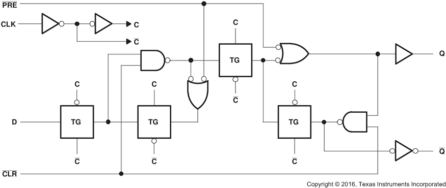
 Logic Diagram, Each Flip-Flop
(Positive Logic)