SCHS245D November   1998  – April 2024 CD54AC245 , CD54ACT245 , CD74AC245 , CD74ACT245

PRODMIX  

  1.   1
  2. Features
  3. Description
  4. Pin Configuration and Functions
  5. Specifications
    1. 4.1 Absolute Maximum Ratings
    2. 4.2 Recommended Operating Conditions
    3. 4.3 Thermal Information
    4. 4.4 Electrical Characteristics
    5. 4.5 Switching Characteristics
    6. 4.6 Timing Diagrams
  6. Parameter Measurement Information
  7. Detailed Description
    1. 6.1 Overview
    2. 6.2 Functional Block Diagram
    3. 6.3 Device Functional Modes
  8. Application and Implementation
    1. 7.1 Power Supply Recommendations
    2. 7.2 Layout
      1. 7.2.1 Layout Guidelines
      2. 7.2.2 Layout Example
  9. Device and Documentation Support
    1. 8.1 Documentation Support
      1. 8.1.1 Related Links
    2. 8.2 Receiving Notification of Documentation Updates
    3. 8.3 Support Resources
    4. 8.4 Trademarks
    5. 8.5 Electrostatic Discharge Caution
    6. 8.6 Glossary
  10. Revision History
  11. 10Mechanical, Packaging, and Orderable Information

Timing Diagrams

GUID-20230202-SS0I-NVCM-GKCB-CSWLKNDHPL5K-low.png

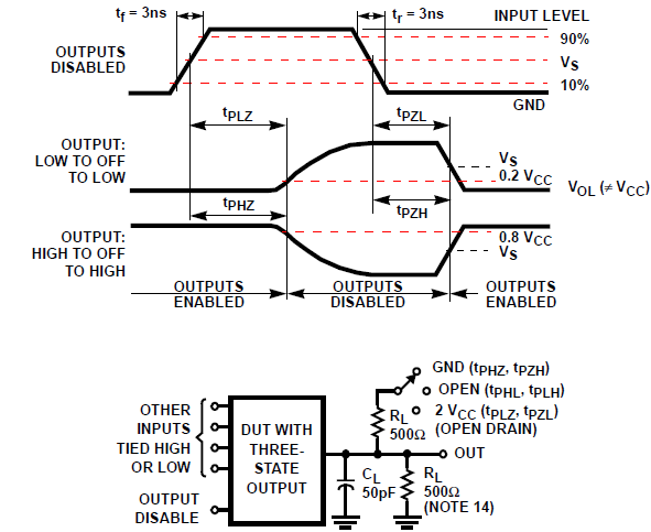
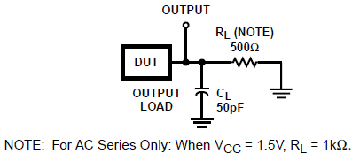
GUID-20230202-SS0I-DDTV-047H-49P5M3GPJDSV-low.png Figure 4-1 THREE-STATE PROPAGATION DELAY TIMES AND TEST CIRCUIT
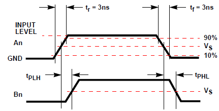
Figure 4-1 SIMULTANEOUS SWITCHING TRANSIENT WAVEFORMS
GUID-20230202-SS0I-NVCM-GKCB-CSWLKNDHPL5K-low.png Figure 4-3 PROPAGATION DELAY TIMES
GUID-20230202-SS0I-WD3X-CJMK-FRVXQ3DX47QM-low.png

Table 4-1
AC ACT
Input Level VCC 3V
Input Switching Voltage, VS 0.5 VCC 1.5V
Output Switching Voltage, VS 0.5 VCC 0.5 VCC

Figure 4-4 PROPAGATION DELAY TIMES