SCHS246A August   1998  – August 2024 CD74AC251

PRODUCTION DATA  

  1.   1
  2. Features
  3. Description
  4. Pin Configuration and Functions
  5. Specifications
    1. 4.1 Absolute Maximum Ratings
    2. 4.2 Recommended Operating Conditions
    3. 4.3 Thermal Information
    4. 4.4 Electrical Characteristics
    5. 4.5 Switching Characteristics
  6. Parameter Measurement Information
  7. Detailed Description
    1. 6.1 Functional Block Diagram
    2. 6.2 Device Functional Modes
  8. Application and Implementation
    1. 7.1 Power Supply Recommendations
    2. 7.2 Layout
      1. 7.2.1 Layout Guidelines
  9. Device and Documentation Support
    1. 8.1 Documentation Support (Analog)
      1. 8.1.1 Related Links
    2. 8.2 Receiving Notification of Documentation Updates
    3. 8.3 Support Resources
    4. 8.4 Trademarks
    5. 8.5 Electrostatic Discharge Caution
    6. 8.6 Glossary
  10. Revision History
  11. 10Mechanical, Packaging, and Orderable Information

Parameter Measurement Information

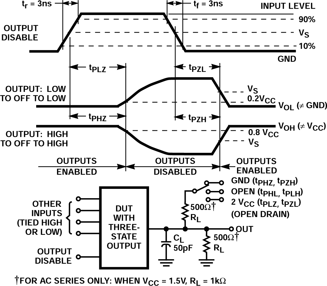
CD74AC251 Three-state Propagation Delay
                    Waveforms and Test Circuit

(1)

Figure 5-1 Three-state Propagation Delay Waveforms and Test Circuit
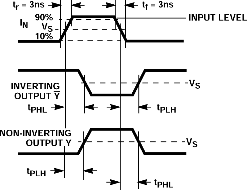
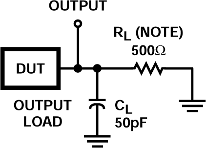
CD74AC251 Propagation Delay TimesFigure 5-2 Propagation Delay Times
CD74AC251 Propagation Delay Times
For AC Series Only: When VCC = 1.5V, RL = 1kΩ.
Figure 5-3 Propagation Delay Times
CD74AC
Input Level VCC
Input Switching Voltage, VS 0.5 VCC
Output Switching Voltage, VS 0.5 VCC
FOR AC SERIES ONLY: WHEN VCC = 1.5V, RL = 1kΩ