SCHS249C November   1998  – May 2024 CD54AC273 , CD54ACT273 , CD74AC273 , CD74ACT273

PRODUCTION DATA  

  1.   1
  2. Features
  3. Description
  4. Pin Configuration and Functions
  5. Specifications
    1. 4.1 Absolute Maximum Ratings
    2. 4.2 ESD Ratings
    3. 4.3 Recommended Operating Conditions
    4. 4.4 Thermal Information
    5. 4.5 Electrical Characteristics
    6. 4.6 Prerequisite for Switching Function
    7. 4.7 Switching Characteristics
  6. Parameter Measurement Information
  7. Detailed Description
    1. 6.1 Overview
    2. 6.2 Functional Block Diagram
    3. 6.3 Device Functional Modes
  8. Application and Implementation
    1. 7.1 Power Supply Recommendations
    2. 7.2 Layout
      1. 7.2.1 Layout Guidelines
  9. Device and Documentation Support
    1. 8.1 Documentation Support (Analog)
      1. 8.1.1 Related Documentation
    2. 8.2 Receiving Notification of Documentation Updates
    3. 8.3 Support Resources
    4. 8.4 Trademarks
    5. 8.5 Electrostatic Discharge Caution
    6. 8.6 Glossary
  10. Revision History
  11. 10Mechanical, Packaging, and Orderable Information

Parameter Measurement Information

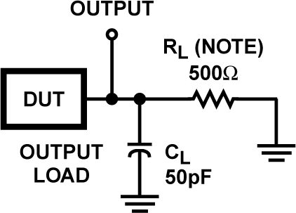
Load Circuit and Voltage Waveforms
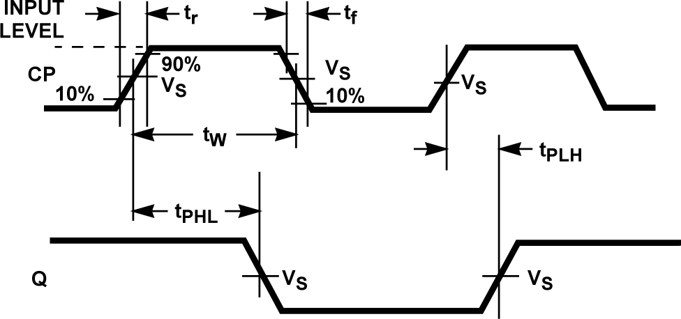
CD54AC273 CD74AC273 CD54ACT273 CD74ACT273 Propagation Delay Times and Clock Pulse Width Propagation Delay Times and Clock Pulse Width
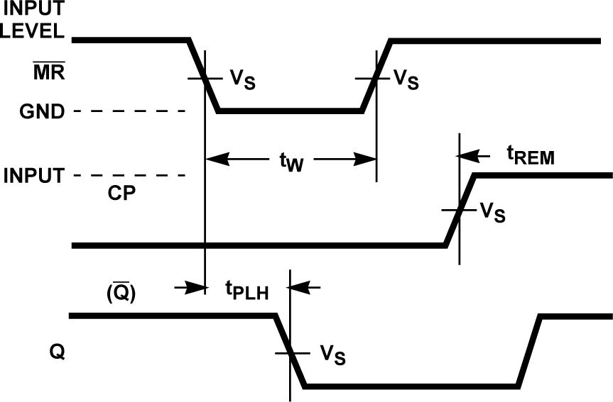
CD54AC273 CD74AC273 CD54ACT273 CD74ACT273 Prerequisite and Propagation Delay Times for Master
                                        Reset Prerequisite and Propagation Delay Times for Master Reset
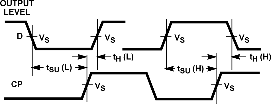
CD54AC273 CD74AC273 CD54ACT273 CD74ACT273 Prerequisite for Clock Prerequisite for Clock
CD54AC273 CD74AC273 CD54ACT273 CD74ACT273 Propagation Delay Times
For AC Series Only: When VCC = 1.5V, RL = 1kΩ.
Propagation Delay Times
AC ACT
Input Level VCC 3V
Input Switching Voltage, VS 0.5 VCC 1.5V
Output Switching Voltage, VS 0.5 VCC 0.5 VCC