SCHS249C November 1998 – May 2024 CD54AC273 , CD54ACT273 , CD74AC273 , CD74ACT273
PRODUCTION DATA
2 Description
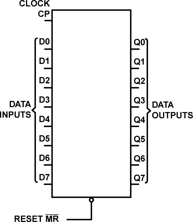
The ’AC273 and ’ACT273 devices are octal D-type flip-flops with reset that utilize advanced CMOS logic technology. Information at the D input is transferred to the Q output on the positive-going edge of the clock pulse. All eight flip-flops are controlled by a common clock (CP) and a common reset (MR). Resetting is accomplished by a low voltage level independent of the clock.
Device Information
| PART NUMBER | PACKAGE(1) | PACKAGE SIZE(2) | BODY SIZE(3) |
|---|---|---|---|
| CD74AC273/ CD74ACT273 | DW (SOIC, 20) | 12.8 mm x 10.3 mm | 12.8 mm x 7.5 mm |
| DB (SSOP, 20) | 7.2 mm x 7.8 mm | 7.2 mm x 5.3 mm | |
| N (PDIP, 20) | 24.33 mm x 9.4 mm | 24.33 mm x 6.35 mm | |
| PW (TSSOP, 20) | 5.00 mm x 6.4 mm | 5.00 mm x 4.4 mm |
(1) For more information, see Section 10.
(2) The package size (length × width)
is a nominal value and includes pins, where applicable.
(3) The body size (length × width) is
a nominal value and does not include pins.
 Functional Block Diagram