SCHS292A December 1998 – May 2024 CD54AC574 , CD54ACT574 , CD74AC574 , CD74ACT574
PRODUCTION DATA
- 1
- 1 Features
- 2 Description
- 3 Pin Configuration and Functions
-
4 Specifications
- 4.1 Absolute Maximum Ratings
- 4.2 ESD Ratings
- 4.3 Recommended Operating Conditions
- 4.4 Thermal Information
- 4.5 Static Electrical Characteristics: AC Series
- 4.6 Static Electrical Characteristics: ACT Series
- 4.7 Prerequisite for Switching: AC Series
- 4.8 Switching Characteristics: AC Series
- 4.9 Prerequisite for Switching: ACT Series
- 4.10 Switching Characteristics: ACT Series
- 5 Parameter Measurement Information
- 6 Detailed Description
- 7 Application and Implementation
- 8 Device and Documentation Support
- 9 Revision History
- 10Mechanical, Packaging, and Orderable Information
2 Description
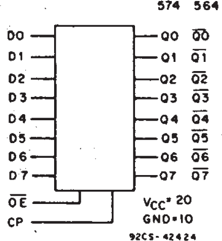
The CDx4AC574 and the CDx4ACT574 octal D-type, 3-state, positive-edge-triggered flip-flops use the RCA ADVANCED CMOS technology.
Device Information
| PART NUMBER | PACKAGE(1) | PACKAGE SIZE(2) | BODY SIZE(3) |
|---|---|---|---|
| CDx4AC/ACT574 | DW (SOIC, 20) | 12.80mm × 10.3mm | 12.80mm × 7.50mm |
| N (PDIP, 20) | 24.33mm × 9.4mm | 24.33mm × 6.35mm |
(1) For all available packages, see
Section 10.
(2) The package size (length × width)
is a nominal value and includes pins, where applicable.
(3) The body size (length × width) is
a nominal value and does not include pins.
 Functional Block
Diagram