SCHS344B April   2003  – October 2024 CD54ACT174 , CD74ACT174

PRODUCTION DATA  

  1.   1
  2. Features
  3. Applications
  4. Description
  5. Pin Configuration and Functions
  6. Specifications
    1. 5.1 Absolute Maximum Ratings
    2. 5.2 ESD Ratings
    3. 5.3 Recommended Operating Conditions
    4. 5.4 Thermal Information
    5. 5.5 Electrical Characteristics
    6. 5.6 Timing Requirements
    7. 5.7 Switching Characteristics
    8. 5.8 Operating Characteristics
  7. Parameter Measurement Information
  8. Detailed Description
    1. 7.1 Overview
    2. 7.2 Functional Block Diagram
    3. 7.3 Device Functional Modes
  9. Application and Implementation
    1. 8.1 Power Supply Recommendations
    2. 8.2 Layout
      1. 8.2.1 Layout Guidelines
      2. 8.2.2 Layout Example
  10. Device and Documentation Support
    1. 9.1 Documentation Support (Analog)
      1. 9.1.1 Related Documentation
    2. 9.2 Receiving Notification of Documentation Updates
    3. 9.3 Support Resources
    4. 9.4 Trademarks
    5. 9.5 Electrostatic Discharge Caution
    6. 9.6 Glossary
  11. 10Revision History
  12. 11Mechanical, Packaging, and Orderable Information

Description

The 'ACT174 devices are positive-edge-triggered D-type flip-flops with a direct clear (CLR) input and are designed for 4.5V to 5.5V VCC operation.

Device Information
PART NUMBER PACKAGE(1) PACKAGE SIZE(2) BODY SIZE(3)
CDx4ACT174 BQB (WQFN, 16) 3.5mm × 2.5mm 3.5mm × 2.5mm
D (SOIC, 16) 9.9mm × 6mm 9.9mm × 3.9mm
N (PDIP, 16) 19.3mm × 9.4mm 19.3mm × 6.35mm
PW (TSSOP, 16) 5mm x 6.4mm 5mm x 4.4mm
For more information, see Section 11.
The package size (length × width) is a nominal value and includes pins, where applicable.
The body size (length × width) is a nominal value and does not include pins.
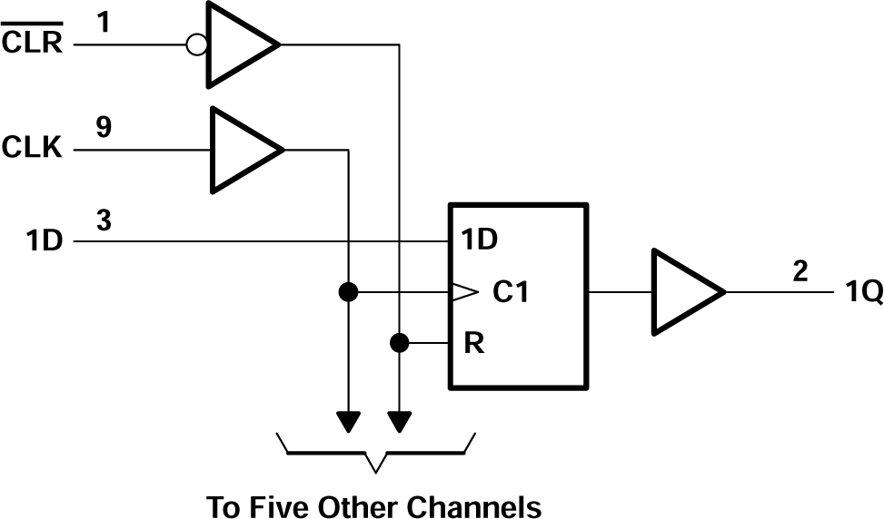
CD54ACT174 CD74ACT174 Logic Diagram (Positive
                        Logic)Logic Diagram (Positive Logic)