SCHS345A April   2003  – May 2024 CD74ACT175

PRODUCTION DATA  
  1.   1
  2. Features
  3. Applications
  4. Description
  5. Pin Configurations and Functions
  6. Specifications
    1. 5.1 Absolute Maximum Ratings
    2. 5.2 ESD Ratings
    3. 5.3 Recommended Operating Conditions
    4. 5.4 Thermal Information
    5. 5.5 Electrical Characteristics
    6. 5.6 Timing Requirements
    7. 5.7 Switching Characteristics
    8. 5.8 Operating Characteristics
  7. Parameter Measurement Information
  8. Detailed Description
    1. 7.1 Overview
    2. 7.2 Functional Block Diagram
    3. 7.3 Device Functional Modes
  9. Application and Implementation
    1. 8.1 Power Supply Recommendations
    2. 8.2 Layout
      1. 8.2.1 Layout Guidelines
  10. Device and Documentation Support
    1. 9.1 Documentation Support (Analog)
      1. 9.1.1 Related Documentation
    2. 9.2 Receiving Notification of Documentation Updates
    3. 9.3 Support Resources
    4. 9.4 Trademarks
    5. 9.5 Electrostatic Discharge Caution
    6. 9.6 Glossary
  11. 10Revision History
  12. 11Mechanical, Packaging, and Orderable Information

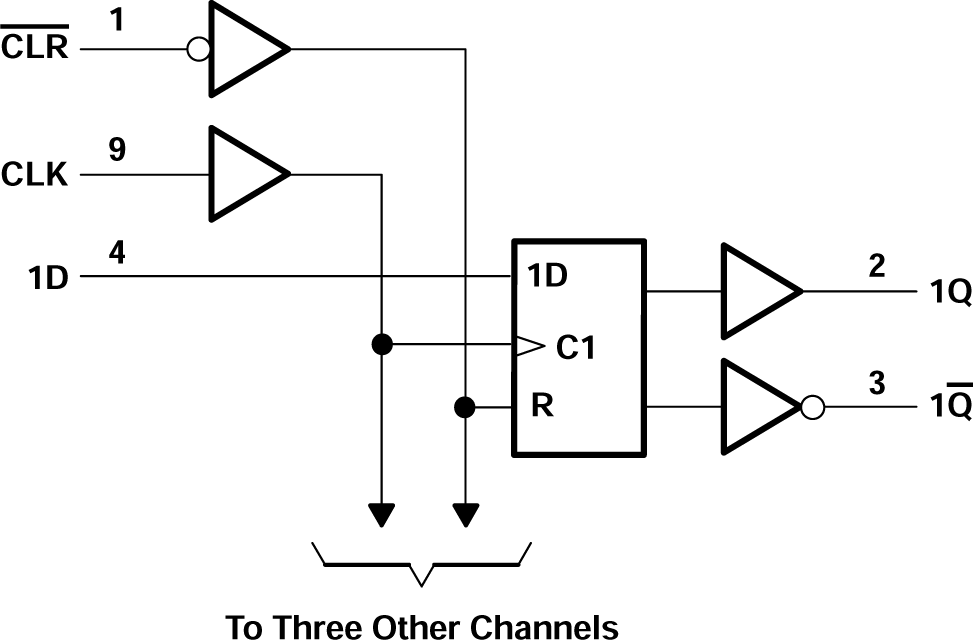
Functional Block Diagram

CD74ACT175 Logic Diagram (Positive Logic) Figure 7-1 Logic Diagram (Positive Logic)