SCHS345A April   2003  – May 2024 CD74ACT175

PRODUCTION DATA  

  1.   1
  2. Features
  3. Applications
  4. Description
  5. Pin Configurations and Functions
  6. Specifications
    1. 5.1 Absolute Maximum Ratings
    2. 5.2 ESD Ratings
    3. 5.3 Recommended Operating Conditions
    4. 5.4 Thermal Information
    5. 5.5 Electrical Characteristics
    6. 5.6 Timing Requirements
    7. 5.7 Switching Characteristics
    8. 5.8 Operating Characteristics
  7. Parameter Measurement Information
  8. Detailed Description
    1. 7.1 Overview
    2. 7.2 Functional Block Diagram
    3. 7.3 Device Functional Modes
  9. Application and Implementation
    1. 8.1 Power Supply Recommendations
    2. 8.2 Layout
      1. 8.2.1 Layout Guidelines
  10. Device and Documentation Support
    1. 9.1 Documentation Support (Analog)
      1. 9.1.1 Related Documentation
    2. 9.2 Receiving Notification of Documentation Updates
    3. 9.3 Support Resources
    4. 9.4 Trademarks
    5. 9.5 Electrostatic Discharge Caution
    6. 9.6 Glossary
  11. 10Revision History
  12. 11Mechanical, Packaging, and Orderable Information

Pin Configurations and Functions

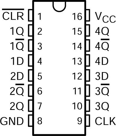
CD74ACT175 D or N Package, 16-PIN
                        SCOIC or PDIP (Top View)Figure 4-1 D or N Package, 16-PIN SCOIC or PDIP (Top View)
Table 4-1 Pin Functions
PIN TYPE DESCRIPTION
NO. NAME
1 CLR I Clear Pin
2 1Q O 1Q Output
3 1Q O 1Q Output
4 1D I 1D Input
5 2D I 2D Input
6 2Q O 2Q Output
7 2Q O 2Q Output
8 GND Ground Pin
9 CLK I Clock Input
10 3Q O 3Q Output
11 3Q O 3QOutput
12 3D I 3D Input
13 4D I 4D Input
14 4Q O 4QOutput
15 4Q O 4Q Output
16 VCC Power Pin