SCHS346C April 2003 – October 2024 CD74AC174
PRODUCTION DATA
- 1
- 1 Features
- 2 Application
- 3 Description
- 4 Pin Configuration and Functions
-
5 Specifications
- 5.1 Absolute Maximum Ratings
- 5.2 ESD Ratings
- 5.3 Recommended Operating Conditions
- 5.4 Thermal Information
- 5.5 Electrical Characteristics
- 5.6 Timing Requirements, VCC = 1.5 V
- 5.7 Timing Requirements, VCC = 3.3 V ± 0.3 V
- 5.8 Timing Requirements, VCC = 5 V ± 0.5 V
- 5.9 Switching Characteristics, VCC = 1.5 V
- 5.10 Switching Characteristics, VCC = 3.3 V ± 0.3 V
- 5.11 Switching Characteristics, VCC = 5 V ± 0.5 V
- 5.12 Operating Characteristics
- 6 Parameter Measurement Information
- 7 Detailed Description
- 8 Application and Implementation
- 9 Device and Documentation Support
- 10Revision History
- 11Mechanical, Packaging, and Orderable Information
3 Description
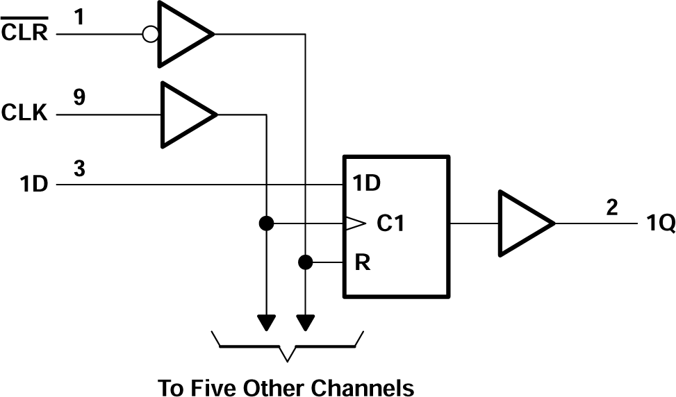
The CD74AC174 is a positive-edge-triggered D-type flip-flop with a direct clear (CLR) input and is designed for 1.5V to 5.5V VCC operation.
Package
Information
| PART NUMBER | PACKAGE(1) | PACKAGE SIZE(2) | BODY SIZE(3) |
|---|---|---|---|
| CD74AC174 | BQB (WQFN, 16) | 3.5mm × 2.5mm | 3.5mm × 2.5mm |
| D (SOIC, 16) | 9.9mm × 6mm | 9.9mm × 3.9mm | |
| N (PDIP, 16) | 19.3mm × 9.4mm | 19.3mm × 6.35mm | |
| PW (TSSOP, 16) | 5mm x 6.4mm | 5mm x 4.4mm |
(1) For more information, see Section
11.
(2) The package size (length × width) is a
nominal value and includes pins, where applicable.
(3) The body size (length × width) is a
nominal value and does not include pins.
