-
Designing a Window Comparator with TI Programmable Logic Devices (TPLD) SCLA075 August 2024 TPLD1201 , TPLD1201-Q1 , TPLD1202 , TPLD1202-Q1
-
Designing a Window Comparator with TI Programmable Logic Devices (TPLD)
Designing a Window Comparator with TI Programmable Logic Devices (TPLD)
1
What is a Window Comparator?
Window comparators trigger when the input voltage is within a range of voltages, as opposed to above or below a single voltage. An example of the behavior of a window comparator is shown in Figure 1. When the input voltage is above 1.7V and below 2V, the window comparator outputs high, and otherwise, it outputs low.
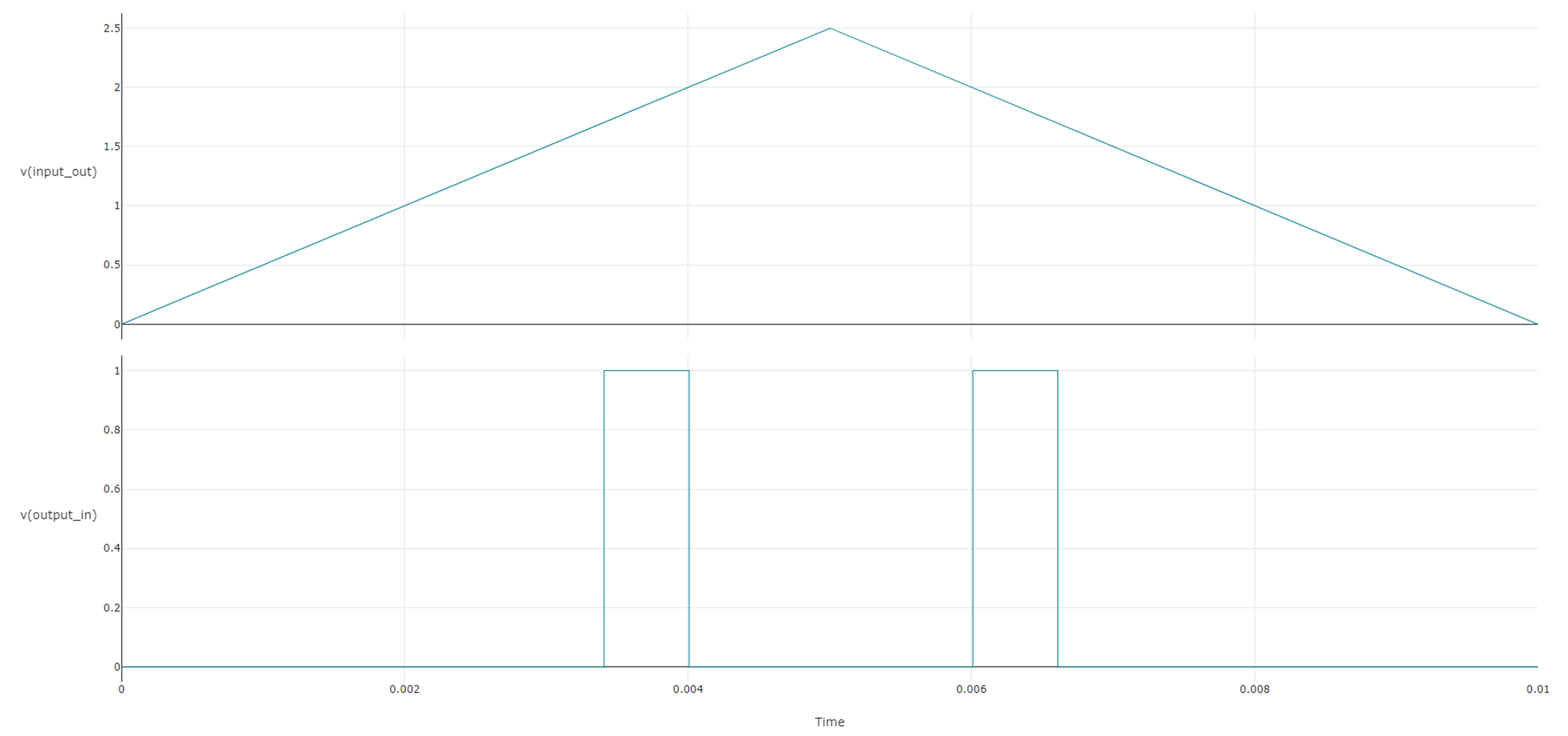 Figure 1 Behavior of a Window Comparator in InterConnect Studio (ICS)
Window comparators are used in a wide array of applications, including temperature sensing and signal processing. They are often used in conjunction with logical elements to manage the output signal. Using TI Programmable Logic Devices (TPLD) , the window comparator and signal handling elements can be combined into a single chip solution, reducing the board space requirements and simplifying the BOM of the system.
How to Configure a Window Comparator in TPLD
Most devices within the TPLD portfolio, such as the TPLD1201 and the TPLD1202, have integrated analog comparators along with their logical elements. Using InterConnect Studio (ICS), the analog comparators can be configured to behave as a window comparator, as shown in Figure 2.
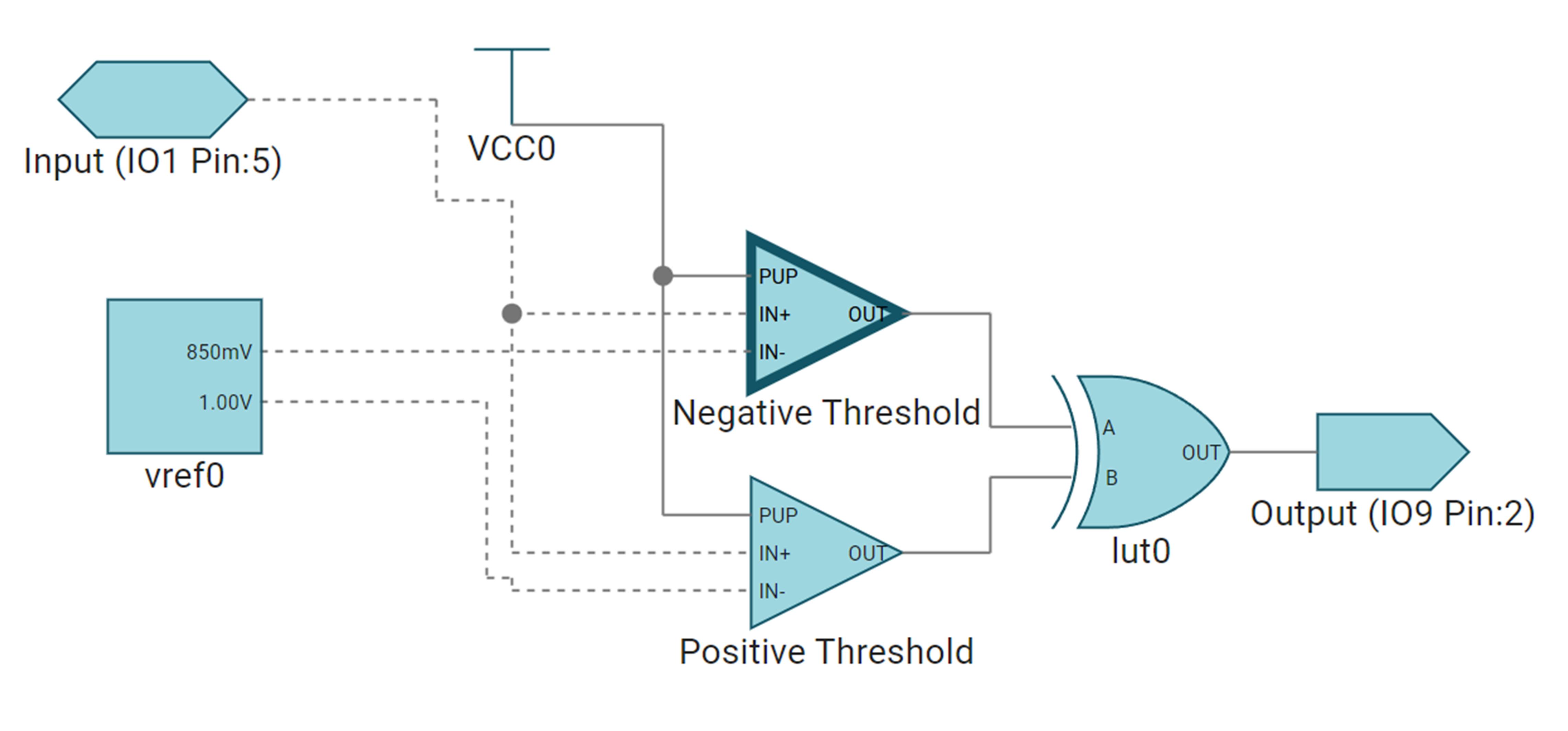 Figure 2 Window Comparator using Internal Voltage References in ICS
In the configuration shown in Figure 2, the outputs of two analog comparators measuring the same voltage are combined using an XOR gate. The output of the gate triggers only when one, but not both, of the analog comparators is above its voltage reference. The negative threshold of the window comparator is set as the lower reference voltage and the positive threshold of the window comparator is set as the higher reference voltage. Figure 1 shows the behavior of this configuration.
In this design, both reference voltages are provided by the TPLD’s internal voltage references. If necessary, one of the reference voltages can instead be set as an external voltage by changing the negative threshold of one of the analog comparators to be an external pin instead of the internal voltage reference, as shown in Figure 3.
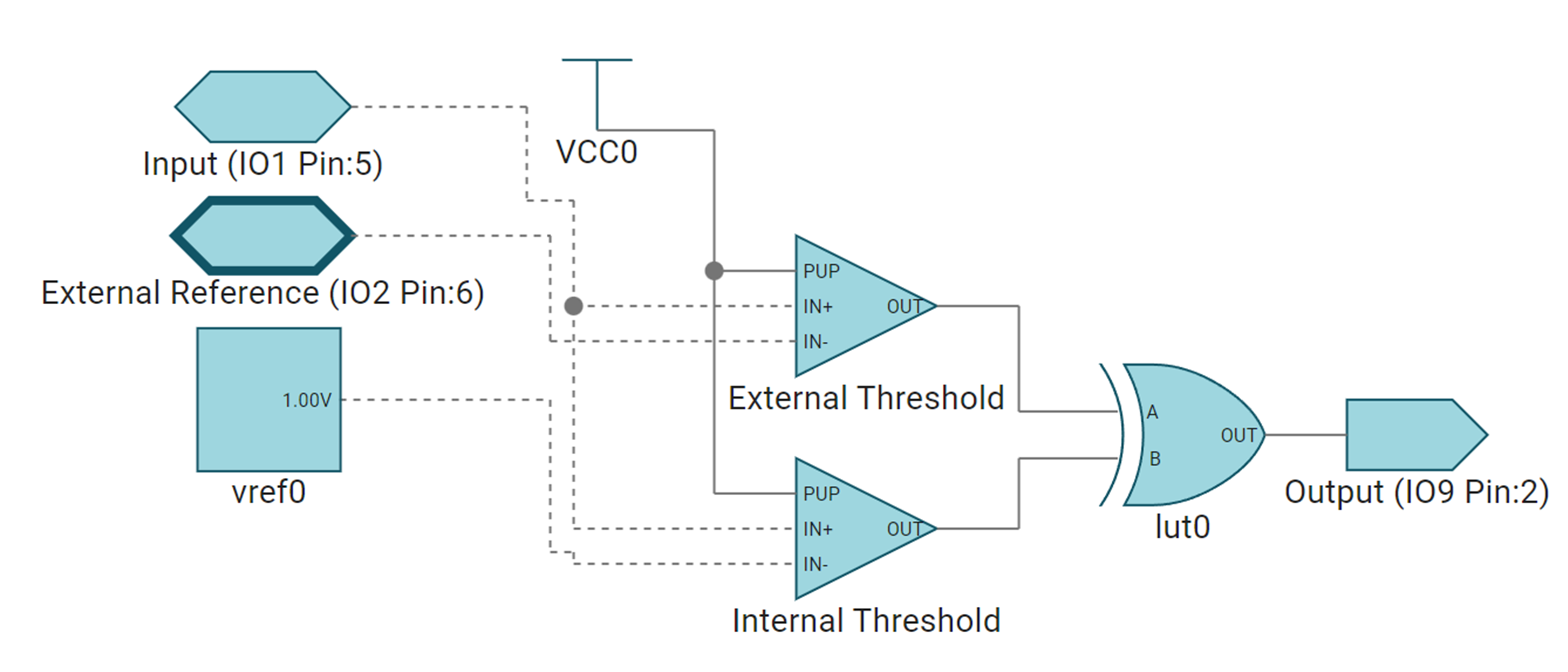 Figure 3 Window Comparator using an External Voltage Reference in ICS
Once the window comparator is configured, the output of the lookup table can be used with the other elements in the TPLD to create an integrated solution. Figure 4 shows an example where a window comparator is used to provide the enable signal to a 1kHz PWM signal with a 25% duty cycle when the input voltage is between 0.5V and 2V.
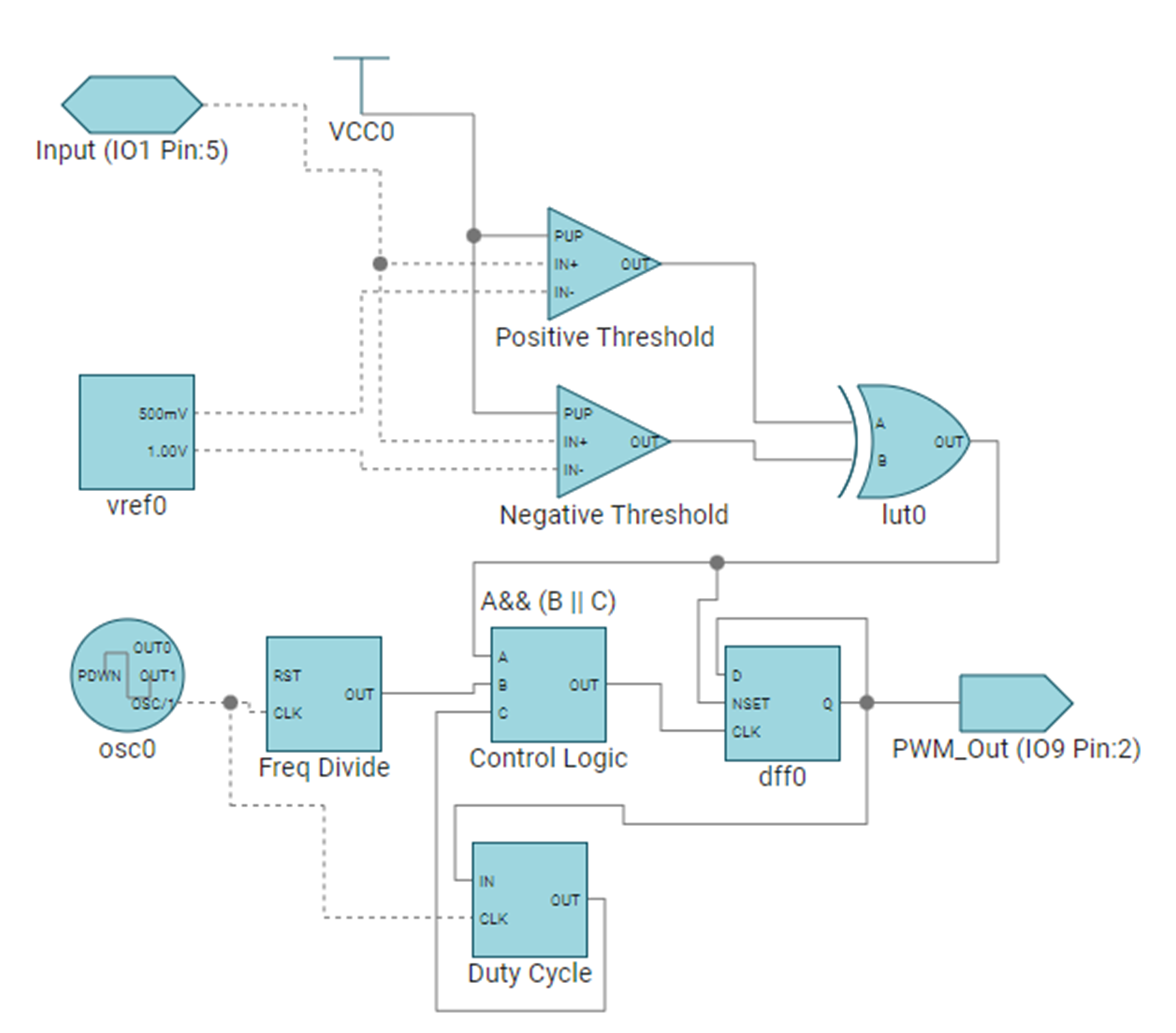 Figure 4 Integrated Window Comparator
and PWM Generator
Figure 4 Integrated Window Comparator
and PWM GeneratorFigure 5 shows the output simulation of this example configuration generated by ICS.
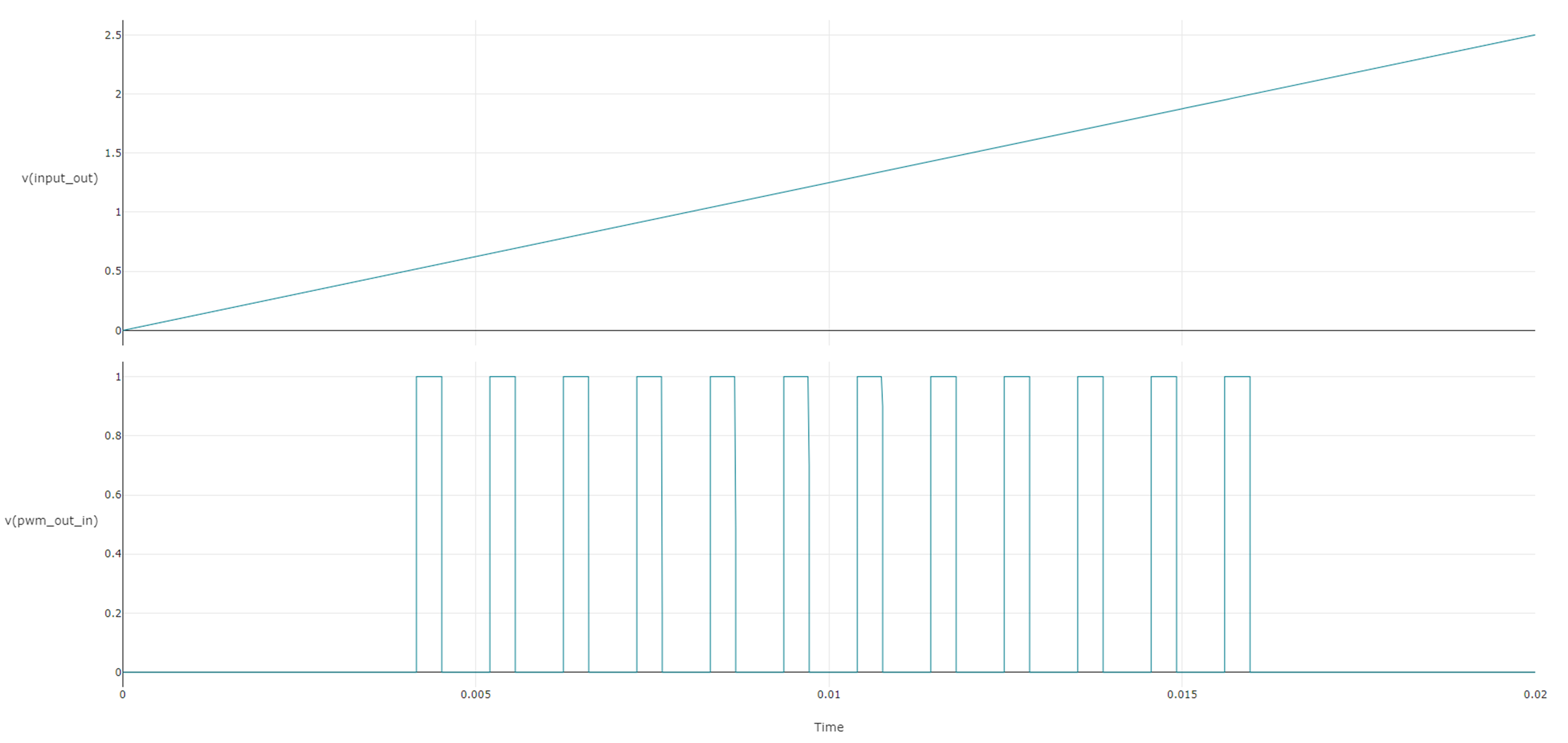 Figure 5 Integrated Window Comparator
and PWM Generator ICS Simulation
Figure 5 Integrated Window Comparator
and PWM Generator ICS SimulationDesign Considerations
TPLD1201 and TPLD1202 do not support input voltages above VCC.
This design outputs a high signal when the input voltage is within the window comparator’s limits. For a design that outputs a low signal when the input voltage is within the limits, switch the XOR gate for an XNOR gate.
The blocks present in TPLD allow for the design and configuration of many complex systems combining digital and analog signals. For more information on TPLD, visit the TPLD1201 product page or ask our engineers a question on the TI E2E™ Logic Support Forum.
Trademarks
All trademarks are the property of their respective owners.
IMPORTANT NOTICE AND DISCLAIMER
TI PROVIDES TECHNICAL AND RELIABILITY DATA (INCLUDING DATASHEETS), DESIGN RESOURCES (INCLUDING REFERENCE DESIGNS), APPLICATION OR OTHER DESIGN ADVICE, WEB TOOLS, SAFETY INFORMATION, AND OTHER RESOURCES “AS IS” AND WITH ALL FAULTS, AND DISCLAIMS ALL WARRANTIES, EXPRESS AND IMPLIED, INCLUDING WITHOUT LIMITATION ANY IMPLIED WARRANTIES OF MERCHANTABILITY, FITNESS FOR A PARTICULAR PURPOSE OR NON-INFRINGEMENT OF THIRD PARTY INTELLECTUAL PROPERTY RIGHTS.
These resources are intended for skilled developers designing with TI products. You are solely responsible for (1) selecting the appropriate TI products for your application, (2) designing, validating and testing your application, and (3) ensuring your application meets applicable standards, and any other safety, security, or other requirements. These resources are subject to change without notice. TI grants you permission to use these resources only for development of an application that uses the TI products described in the resource. Other reproduction and display of these resources is prohibited. No license is granted to any other TI intellectual property right or to any third party intellectual property right. TI disclaims responsibility for, and you will fully indemnify TI and its representatives against, any claims, damages, costs, losses, and liabilities arising out of your use of these resources.
TI’s products are provided subject to TI’s Terms of Sale (www.ti.com/legal/termsofsale.html) or other applicable terms available either on ti.com or provided in conjunction with such TI products. TI’s provision of these resources does not expand or otherwise alter TI’s applicable warranties or warranty disclaimers for TI products.
Mailing Address: Texas Instruments, Post Office Box 655303, Dallas, Texas 75265
Copyright © 2024, Texas Instruments Incorporated