SCLS099I December   1982  – September 2024 SN54HC112 , SN74HC112

PRODUCTION DATA  

  1.   1
  2. Features
  3. Applications
  4. Description
  5. Pin Configuration and Functions
  6. Specifications
    1. 5.1 Absolute Maximum Ratings
    2. 5.2 Recommended Operating Conditions #GUID-2EBD0632-9121-4D73-88A3-4D53587EF83D/GUID-D459A9EC-CCFD-4DD4-8D23-57A07F876135
    3. 5.3 Thermal Information
    4. 5.4 Electrical Characteristics
    5. 5.5 Timing Requirements
    6. 5.6 Switching Characteristics
    7. 5.7 Operating Characteristics
  7. Parameter Measurement Information
  8. Detailed Description
    1. 7.1 Overview
    2. 7.2 Functional Block Diagram
    3. 7.3 Device Functional Modes
  9. Application and Implementation
    1. 8.1 Power Supply Recommendations
    2. 8.2 Layout
      1. 8.2.1 Layout Guidelines
  10. Device and Documentation Support
    1. 9.1 Receiving Notification of Documentation Updates
    2. 9.2 Support Resources
    3. 9.3 Trademarks
    4. 9.4 Electrostatic Discharge Caution
    5. 9.5 Glossary
  11. 10Revision History
  12. 11Mechanical, Packaging, and Orderable Information

Description

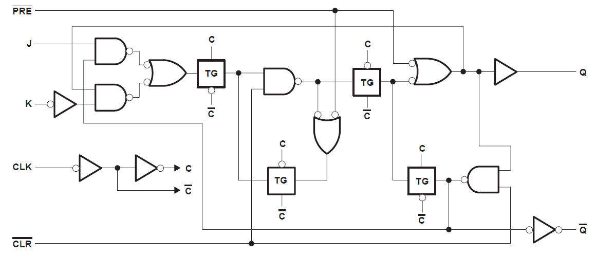
The SNx4HC112 devices contain two independent J-K negative-edge-triggered flip-flops. A low level at the preset (PRE) or clear (CLR) inputs sets or resets the outputs, regardless of the levels of the other inputs. When PRE and CLR are inactive (high), data at the J and K inputs meeting the setup time requirements are transferred to the outputs on the negative-going edge of the clock (CLK) pulse. Clock triggering occurs at a voltage level and is not directly related to the fall time of the CLK pulse. Following the hold-time interval, data at the J and K inputs may be changed without affecting the levels at the outputs. These versatile flip-flops perform as toggle flip-flops by tying J and K high.

Device Information
PART NUMBER PACKAGE(1) PACKAGE SIZE(2) BODY SIZE (NOM)(3)
SNx4HC112 J (CDIP, 16) 19.56mm × 6.92mm 19.56mm × 6.92mm
D (SOIC, 16) 9.9mm × 6mm 9.9mm × 3.9mm
N (PDIP, 16) 19.3mm × 9.4mm 19.3mm × 6.35mm
FK (LCCC, 20) 8.89mm × 8.89mm 8.89mm × 8.89mm
W (CFP, 16) 10.3mm × 6.73mm 10.3mm × 6.73mm
For more information, see Section 11
The package size (length × width) is a nominal value and includes pins, where applicable.
The body size (length × width) is a nominal value and does not include pins.
SN54HC112 SN74HC112 Functional Block
                                                  Diagram Functional Block Diagram