SCLS177H March 1984 – August 2024 SN74HCT574
PRODUCTION DATA
2 Description
These octal edge-triggered D-type flip-flops feature 3-state outputs designed specifically for bus driving. The ’HCT574 devices are particularly suitable for implementing buffer registers, I/O ports, bidirectional bus drivers, and working registers.
Device
Information
| PART NUMBER | PACKAGE(1) | PACKAGE SIZE(2) | BODY SIZE(3) |
|---|---|---|---|
| SN74HCT574 | DGS (VSSOP, 20) | 5.1mm × 4.9mm | 5.1mm × 3mm |
| DW (SOIC, 20) | 12.80mm x 10.3mm | 12.80mm x 7.50mm | |
| DB (SSOP, 20) | 7.2mm x 7.8mm | 7.2mm x 5.30mm | |
| PDIP (20) | 24.33mm × 9.4mm | 24.33mm × 6.35mm | |
| NS (SOP, 20) | 12.6mm x 7.8mm | 12.6mm x 5.3mm | |
| PW (TSSOP, 20) | 6.50mm x 6.4mm | 6.50mm x 4.40mm |
(1) For more information, see Section 11.
(2) The package size (length × width) is a nominal value and
includes pins, where applicable.
(3) The body size (length × width) is a nominal value and
does not include pins.
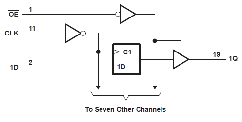
 Logic Diagram (Positive Logic)