SCLS226L October 1995 – July 2024 SN54AHC244 , SN54AHC244-SP , SN74AHC244
PRODUCTION DATA
- 1
- 1 Features
- 2 Applications
- 3 Description
- 4 Pin Configuration and Functions
-
5 Specifications
- 5.1 Absolute Maximum Ratings
- 5.2 ESD Ratings
- 5.3 Recommended Operating Conditions
- 5.4 Thermal Information
- 5.5 Electrical Characteristics
- 5.6 Switching Characteristics, VCC = 3.3V ± 0.3V
- 5.7 Switching Characteristics, VCC = 5V ± 0.5V
- 5.8 Noise Characteristics
- 5.9 Operating Characteristics
- 5.10 Typical Characteristics
- 6 Parameter Measurement Information
- 7 Detailed Description
- 8 Application and Implementation
- 9 Device and Documentation Support
- 10Revision History
- 11Mechanical, Packaging, and Orderable Information
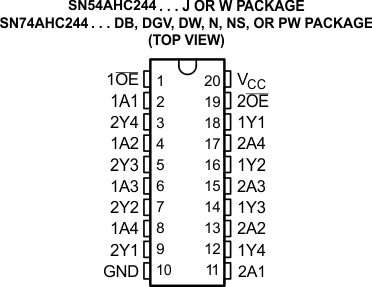
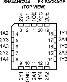
4 Pin Configuration and Functions


Table 4-1 Pin Functions
| PIN | I/O | DESCRIPTION | |
|---|---|---|---|
| NO. | NAME | ||
| 1 | 1 OE | I | Output Enable 1 |
| 2 | 1A1 | I | 1A1 Input |
| 3 | 2Y4 | O | 2Y4 Output |
| 4 | 1A2 | I | 1A2 Input |
| 5 | 2Y3 | O | 2Y3 Output |
| 6 | 1A3 | I | 1A3 Input |
| 7 | 2Y2 | O | 2Y2 Output |
| 8 | 1A4 | I | 1A4 Input |
| 9 | 2Y1 | O | 2Y1 Output |
| 10 | GND | — | Ground pin |
| 11 | 2A1 | I | 2A1 Input |
| 12 | 1Y4 | O | 1Y4 Output |
| 13 | 2A2 | I | 2A2 Input |
| 14 | 1Y3 | O | 1Y3 Output |
| 15 | 2A3 | I | 2A3 Input |
| 16 | 1Y2 | O | 1Y2 Output |
| 17 | 2A4 | I | 2A4 Input |
| 18 | 1Y1 | O | 1Y1 Output |
| 19 | 2 OE | I | Output Enable 2 |
| 20 | VCC | — | Power Pin |