SCLS243Q October 1995 – July 2024 SN54AHCT573 , SN74AHCT573
PRODUCTION DATA
- 1
- 1 Features
- 2 Applications
- 3 Description
- 4 Pin Configuration and Functions
-
5 Specifications
- 5.1 Absolute Maximum Ratings
- 5.2 ESD Ratings
- 5.3 Recommended Operating Conditions
- 5.4 Thermal Information
- 5.5 Electrical Characteristics
- 5.6 Timing Requirements
- 5.7 Switching Characteristics, SNx4AHCT573
- 5.8 Switching Characteristics, SN54AHCT573
- 5.9 Operating Characteristics
- 5.10 Typical Characteristics
- 6 Parameter Measurement Information
- 7 Detailed Description
- 8 Application and Implementation
- 9 Device and Documentation Support
- 10Revision History
- 11Mechanical, Packaging, and Orderable Information
3 Description
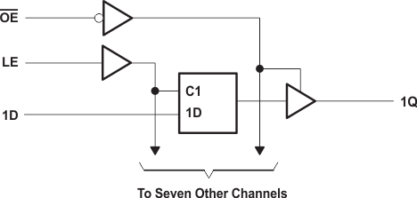
The SNx4AHCT573 devices are octal transparent D-type latches. When the latch-enable (LE) input is high, the Q outputs follow the data (D) inputs. When LE is low, the Q outputs are latched at the logic levels of the D inputs.
Device Information
| PART NUMBER | RATING(1) | PACKAGE(1) |
|---|---|---|
| SN74AHCT573 | Catalog | DB (SSOP, 20) |
| DGV (TVSOP, 20) | ||
| DW (SOIC, 20) | ||
| N (PDIP, 20) | ||
| PW (TSSOP, 20) | ||
| SN54AHCT573 | Military | J (CDIP, 20) |
| W (CFP, 20) |
(1) For more information, see Section 11.
 Simplified Schematic