SCLS259M December 1995 – July 2024 SN74AHC139
PRODUCTION DATA
- 1
- 1 Features
- 2 Description
- 3 Pin Configuration and Functions
- 4 Specifications
- 5 Parameter Measurement Information
- 6 Detailed Description
- 7 Application and Implementation
- 8 Device and Documentation Support
- 9 Revision History
- 10Mechanical, Packaging, and Orderable Information
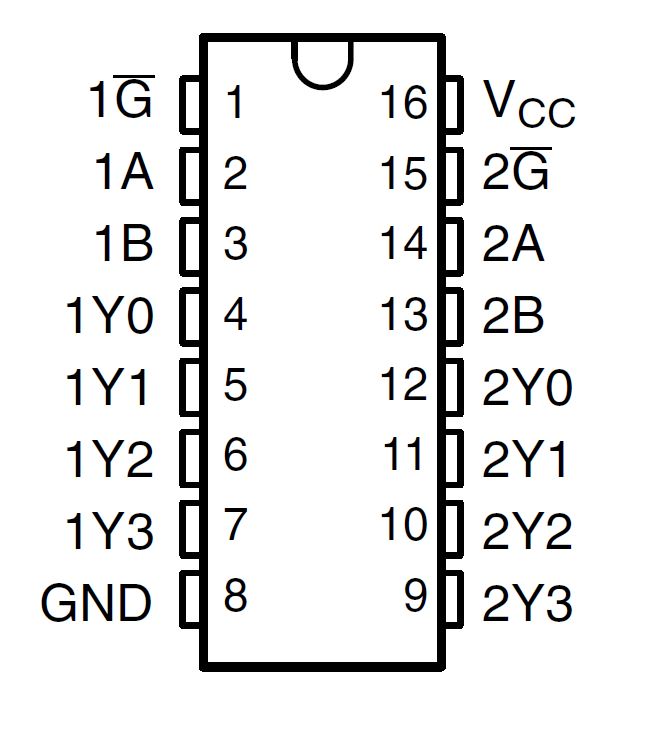
3 Pin Configuration and Functions
 Figure 3-1 SN74AHC139 D, DB, DGV, N, NS, or PW
Package (Top View)
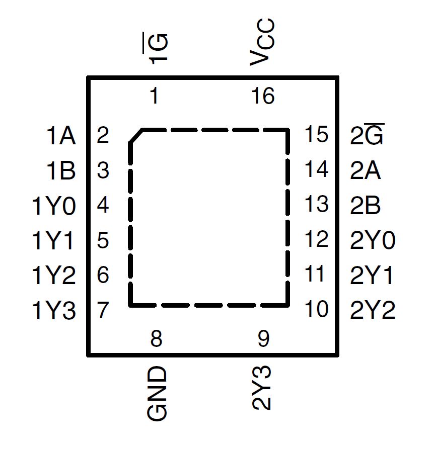
 Figure 3-2 SN74AHC139 RGY Package (Top
View)
Figure 3-2 SN74AHC139 RGY Package (Top
View)Table 3-1 Pin Functions
| PIN | TYPE(1) | DESCRIPTION | |
|---|---|---|---|
| NAME | D, DB, DGV, N, NS, PW, RGY | ||
| NC | — |
I |
Output enable input 1, active low |
| 1G | 1 |
I |
Input for channel 1 |
| 1A | 2 |
I |
Input for channel 2 |
| 1B | 3 |
I |
Input for channel 3 |
| 1Y0 | 4 |
I |
Input for channel 4 |
| NC | — |
I |
Input for channel 5 |
| 1Y1 | 5 |
I |
Input for channel 6 |
| 1Y2 | 6 |
I |
Input for channel 7 |
| 1Y3 | 7 |
I |
Input for channel 8 |
| GND | 8 |
G |
Ground |
| NC | — |
O |
Output for channel 8 |
| 2Y3 | 9 |
O |
Output for channel 7 |
| 2Y2 | 10 |
O |
Output for channel 6 |
| 2Y1 | 11 | O | Output for channel 5 |
| 2Y0 | 12 | O | Output for channel 4 |
| NC | — | O | Output for channel 3 |
| 2B | 13 | O | Output for channel 2 |
| 2A | 14 | O | Output for channel 1 |
| 2G | 15 | I | Output enable input 2, active low |
| VCC | 16 | P | Positive supply |
(1) Signal Types: I = Input, O = Output, I/O
= Input or Output.