SCLS510D June   2003  – October 2024 SN74AHCT1G04-Q1

PRODUCTION DATA  

  1.   1
  2. Features
  3. Applications
  4. Description
  5. Pin Configuration and Functions
  6. Specifications
    1. 5.1 Absolute Maximum Ratings
    2. 5.2 ESD Ratings
    3. 5.3 Recommended Operating Conditions
    4. 5.4 Thermal Information
    5. 5.5 Electrical Characteristics
    6. 5.6 Switching Characteristics
    7. 5.7 Operating Characteristics
    8. 5.8 Typical Characteristics
  7. Parameter Measurement Information
    1. 6.1 16
  8. Detailed Description
    1. 7.1 Functional Block Diagram
    2. 7.2 Device Functional Modes
  9. Device and Documentation Support
    1. 8.1 Documentation Support
      1. 8.1.1 Related Documentation
    2. 8.2 Receiving Notification of Documentation Updates
    3. 8.3 Support Resources
    4. 8.4 Trademarks
    5. 8.5 Electrostatic Discharge Caution
    6. 8.6 Glossary
  10. Revision History
  11. 10Mechanical, Packaging, and Orderable Information

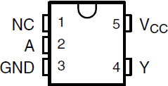
Pin Configuration and Functions

SN74AHCT1G04-Q1 DBV Package, 5-Pin SOT-23; DCK
            Package (Top View)Figure 4-1 DBV Package, 5-Pin SOT-23; DCK Package (Top View)
SN74AHCT1G04-Q1 DTX Package, 5-Pin X2SON (Top
            View)

NC − No internal connection

Figure 4-2 DTX Package, 5-Pin X2SON (Top View)
Table 4-1 Pin Functions
PIN TYPE DESCRIPTION
NO. NAME
1 NC No Connection
2 A I Input A
3 GND Ground Pin
4 Y O Output Y
5 VCC Power Pin