SCLS581C April   2004  – July 2024 CD74HCT4066-Q1

PRODUCTION DATA  

  1.   1
  2. Features
  3. Applications
  4. Description
  5. Pin Configuration and Functions
  6. Specifications
    1. 5.1 Absolute Maximum Ratings
    2. 5.2 Thermal Information
    3. 5.3 Recommended Operating Conditions
    4. 5.4 Electrical Characteristics
    5. 5.5 HCT Input Loading
    6. 5.6 Switching Characteristics
    7. 5.7 Operating Characteristics
    8. 5.8 Analog Channel Characteristics
    9. 5.9 Typical Characteristics
  7. Parameter Measurement Information
  8. Detailed Description
    1. 7.1 Functional Block Diagram
    2. 7.2 Device Functional Modes
  9. Device and Documentation Support
    1. 8.1 Receiving Notification of Documentation Updates
    2. 8.2 Support Resources
    3. 8.3 Trademarks
    4. 8.4 Electrostatic Discharge Caution
    5. 8.5 Glossary
  10. Revision History
  11. 10Mechanical, Packaging, and Orderable Information

Description

The CD74HCT4066-Q1 contains four independent digitally controlled analog switches that use silicon-gate CMOS technology to achieve operation speeds similar to LSTTL, with the low power consumption of standard CMOS integrated circuits.

These switches feature the characteristic linear ON resistance of the metal-gate CD4066B. Each switch is turned on by a high-level voltage on its control input.

Package Information
PART NUMBERPACKAGE(1)PACKAGE SIZE(2)
CD74HCT4066-Q1PW (TSSOP, 14)5mm × 6.4mm
For more information, see Section 10
The package size (length × width) is a nominal value and includes pins, where applicable.
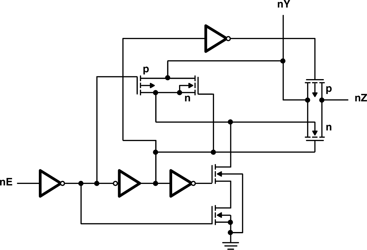
CD74HCT4066-Q1 Logic Diagram (Positive Logic)Logic Diagram (Positive Logic)