SCLS740D November   2013  – August 2024 SN74LV1T02

PRODUCTION DATA  

  1.   1
  2. Features
  3. Applications
  4. Description
  5. Related Products
  6. Pin Configuration and Functions
  7. Specifications
    1. 6.1 Absolute Maximum Ratings
    2. 6.2 ESD Ratings
    3. 6.3 Recommended Operating Conditions
    4. 6.4 Thermal Information
    5. 6.5 Electrical Characteristics
    6. 6.6 Switching Characteristics
    7. 6.7 Operating Characteristics
    8. 6.8 Typical Characteristics
  8. Parameter Measurement Information
  9. Detailed Description
    1. 8.1 Overview
    2. 8.2 Functional Block Diagram
    3. 8.3 Feature Description
      1. 8.3.1 Clamp Diode Structure
      2. 8.3.2 Balanced CMOS Push-Pull Outputs
      3. 8.3.3 LVxT Enhanced Input Voltage
        1. 8.3.3.1 Down Translation
        2. 8.3.3.2 Up Translation
    4. 8.4 Device Functional Modes
  10. Application and Implementation
    1. 9.1 Power Supply Recommendations
    2. 9.2 Layout
      1. 9.2.1 Layout Guidelines
      2. 9.2.2 Layout Example
  11. 10Device and Documentation Support
    1. 10.1 Receiving Notification of Documentation Updates
    2. 10.2 Support Resources
    3. 10.3 Trademarks
    4. 10.4 Electrostatic Discharge Caution
    5. 10.5 Glossary
  12. 11Revision History
  13. 12Mechanical, Packaging, and Orderable Information

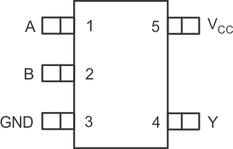
Pin Configuration and Functions

SN74LV1T02 DCK
                                                  or DBV Package, 5-Pin SC70 or SOT-23 (Top
                                                  View) Figure 5-1 DCK or DBV Package, 5-Pin SC70 or SOT-23 (Top View)
Table 5-1 Pin Functions
PINTYPE(1)DESCRIPTION
NAMENO.
A1IInput A
B2IInput B
GND3GGround
Y4OOutput Y
VCC5PPositive supply
I = Input, O = Output, I/O = Input or Output, G = Ground, P = Power.