SCLS741D November   2013  – May 2024 SN74LV1T32

PRODUCTION DATA  

  1.   1
  2. Features
  3. Applications
  4. Description
  5. Related Products
  6. Pin Configuration and Functions
  7. Specifications
    1. 6.1 Absolute Maximum Ratings
    2. 6.2 ESD Ratings
    3. 6.3 Recommended Operating Conditions
    4. 6.4 Thermal Information
    5. 6.5 Electrical Characteristics
    6. 6.6 Switching Characteristics
    7. 6.7 Operating Characteristics
    8. 6.8 Typical Characteristics
  8. Parameter Measurement Information
  9. Detailed Description
    1. 8.1 Overview
    2. 8.2 Functional Block Diagram
    3. 8.3 Feature Description
      1. 8.3.1 Clamp Diode Structure
      2. 8.3.2 Balanced CMOS Push-Pull Outputs
      3. 8.3.3 LVxT Enhanced Input Voltage
      4. 8.3.4 Down Translation
      5. 8.3.5 Up Translation
    4. 8.4 Device Functional Modes
  10. Application and Implementation
    1. 9.1 Power Supply Recommendations
    2. 9.2 Layout
      1. 9.2.1 Layout Guidelines
      2. 9.2.2 Layout Example
  11. 10Device and Documentation Support
    1. 10.1 Documentation Support (Analog)
      1. 10.1.1 Related Documentation
    2. 10.2 Receiving Notification of Documentation Updates
    3. 10.3 Support Resources
    4. 10.4 Trademarks
    5. 10.5 Electrostatic Discharge Caution
    6. 10.6 Glossary
  12. 11Revision History
  13. 12Mechanical, Packaging, and Orderable Information

Clamp Diode Structure

The outputs to this device have both positive and negative clamping diodes, and the inputs to this device have negative clamping diodes only as shown in Figure 8-1.

CAUTION: Voltages beyond the values specified in the Absolute Maximum Ratings table can cause damage to the device. The input and output voltage ratings may be exceeded if the input and output clamp-current ratings are observed.
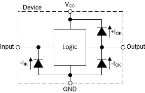
SN74LV1T32 Electrical Placement of Clamping
          Diodes for Each Input and Output Figure 8-1 Electrical Placement of Clamping Diodes for Each Input and Output