SCLS951A August 2023 – November 2023 SN74LV8T165-Q1
PRODUCTION DATA
- 1
- 1 Features
- 2 Applications
- 3 Description
- 4 Pin Configuration and Functions
- 5 Specifications
- 6 Parameter Measurement Information
- 7 Detailed Description
- 8 Application and Implementation
- 9 Device and Documentation Support
- 10Revision History
- 11Mechanical, Packaging, and Orderable Information
4 Pin Configuration and Functions
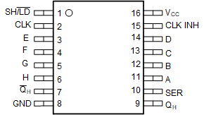
 Figure 4-1 PW Package, 16-Pin TSSOP
(Top View)
 Figure 4-2 BQB Package, 16-Pin WQFN
(Top View)
Figure 4-2 BQB Package, 16-Pin WQFN
(Top View)Table 4-1 Pin Functions
| PIN | TYPE(1) | DESCRIPTION | |
|---|---|---|---|
| NAME | NO. | ||
| SH/LD | 1 | I | Enable shifting when input is high, load data when input is low |
| CLK | 2 | I | Clock, rising edge triggered |
| E | 3 | I | Parallel input E |
| F | 4 | I | Parallel input F |
| G | 5 | I | Parallel input G |
| H | 6 | I | Parallel input H |
| QH | 7 | O | Inverted serial output |
| GND | 8 | G | Ground |
| QH | 9 | O | Serial output |
| SER | 10 | I | Serial input |
| A | 11 | I | Parallel input A |
| B | 12 | I | Parallel input B |
| C | 13 | I | Parallel input C |
| D | 14 | I | Parallel input D |
| CLK INH | 15 | I | Clock inhibit input |
| VCC | 16 | P | Positive supply |
| Thermal pad(2) | — | The thermal pad can be connect to GND or left floating. Do not connect to any other signal or supply. | |
(1) I = Input, O = Output, I/O =
Input or Output, G = Ground, P = Power
(2) BQB package only.