SCLSA21A September   2024  – October 2024 SN74LV8T244-EP

PRODUCTION DATA  

  1.   1
  2. Features
  3. Applications
  4. Description
  5. Pin Configuration and Functions
  6. Specifications
    1. 5.1 Absolute Maximum Ratings
    2. 5.2 ESD Ratings
    3. 5.3 Recommended Operating Conditions
    4. 5.4 Thermal Information
    5. 5.5 Electrical Characteristics
    6. 5.6 Switching Characteristics
    7. 5.7 Typical Characteristics
  7. Parameter Measurement Information
  8. Detailed Description
    1. 7.1 Overview
    2. 7.2 Functional Block Diagram
  9. Feature Description
    1. 8.1 Balanced CMOS 3-State Outputs
    2. 8.2 LVxT Enhanced Input Voltage
    3. 8.3 Clamp Diode Structure
  10. Device Functional Modes
  11. 10Application and Implementation
    1. 10.1 Application Information
    2. 10.2 Typical Application
      1. 10.2.1 Design Requirements
        1. 10.2.1.1 Power Considerations
        2. 10.2.1.2 Input Considerations
        3. 10.2.1.3 Output Considerations
      2. 10.2.2 Detailed Design Procedure
      3. 10.2.3 Application Curves
    3. 10.3 Power Supply Recommendations
    4. 10.4 Layout
      1. 10.4.1 Layout Guidelines
      2. 10.4.2 Layout Example
  12. 11Device and Documentation Support
    1. 11.1 Documentation Support
      1. 11.1.1 Related Documentation
    2. 11.2 Receiving Notification of Documentation Updates
    3. 11.3 Support Resources
    4. 11.4 Trademarks
    5. 11.5 Electrostatic Discharge Caution
    6. 11.6 Glossary
  13. 12Revision History
  14. 13Mechanical, Packaging, and Orderable Information
    1. 13.1 Tape and Reel Information
    2. 13.2 Mechanical Data

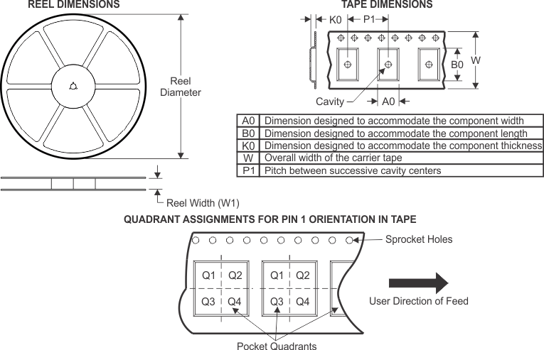
Tape and Reel Information

SN74LV8T244-EP
DevicePackage
Type
Package DrawingPinsSPQReel
Diameter (mm)
Reel
Width W1 (mm)
A0
(mm)
B0
(mm)
K0
(mm)
P1
(mm)
W
(mm)
Pin1
Quadrant
1I8T244MPWREPTSSOPPW202000330.016.46.957.001.48.012.0Q1

SN74LV8T244-EP

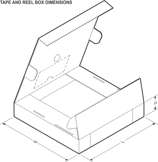
DevicePackage TypePackage DrawingPinsSPQLength (mm)Width (mm)Height (mm)
1I8T244MPWREPTSSOPPW202000367.0367.038.0