SCLSA21A September 2024 – October 2024 SN74LV8T244-EP
PRODUCTION DATA
- 1
- 1 Features
- 2 Applications
- 3 Description
- 4 Pin Configuration and Functions
- 5 Specifications
- 6 Parameter Measurement Information
- 7 Detailed Description
- 8 Feature Description
- 9 Device Functional Modes
- 10Application and Implementation
- 11Device and Documentation Support
- 12Revision History
- 13Mechanical, Packaging, and Orderable Information
4 Pin Configuration and Functions
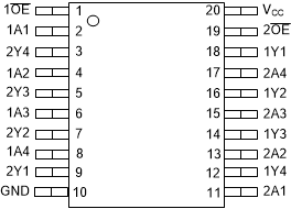
 Figure 4-1 PW Package, 20-Pin TSSOP (Top View)
Table 4-1 Pin Functions
| PIN | TYPE(1) | DESCRIPTION | |
|---|---|---|---|
| NAME | NO. | ||
| 1OE | 1 | I | Bank 1, output enable, active low |
| 1A1 | 2 | I | Bank 1, channel 1 input |
| 2Y4 | 3 | O | Bank 2, channel 4 output |
| 1A2 | 4 | I | Bank 1, channel 2 input |
| 2Y3 | 5 | O | Bank 2, channel 3 output |
| 1A3 | 6 | I | Bank 1, channel 3 input |
| 2Y2 | 7 | O | Bank 2, channel 2 output |
| 1A4 | 8 | I | Bank 1, channel 4 input |
| 2Y1 | 9 | O | Bank 2, channel 1 output |
| GND | 10 | G | Ground |
| 2A1 | 11 | I | Bank 2, channel 1 input |
| 1Y4 | 12 | O | Bank 1, channel 4 output |
| 2A2 | 13 | I | Bank 2, channel 2 input |
| 1Y3 | 14 | O | Bank 1, channel 3 output |
| 2A3 | 15 | I | Bank 2, channel 3 input |
| 1Y2 | 16 | O | Bank 1, channel 2 output |
| 2A4 | 17 | I | Bank 2, channel 4 input |
| 1Y1 | 18 | O | Bank 1, channel 1 output |
| 2OE | 19 | I | Bank 2, output enable, active low |
| VCC | 20 | P | Positive supply |
(1) I = Input, O = Output, I/O = Input or Output, G = Ground, P = Power