SCPS068K July 2001 – September 2024 PCF8574
PRODUCTION DATA
- 1
- 1 Features
- 2 Applications
- 3 Description
- 4 Pin Configuration and Functions
- 5 Specifications
- 6 Parameter Measurement Information
- 7 Detailed Description
- 8 Application and Implementation
- 9 Device and Documentation Support
- 10Revision History
- 11Mechanical, Packaging, and Orderable Information
3 Description
This 8-bit input/output (I/O) expander for the two-line bidirectional bus (I2C) is designed for 2.5V to 6V VCC operation.
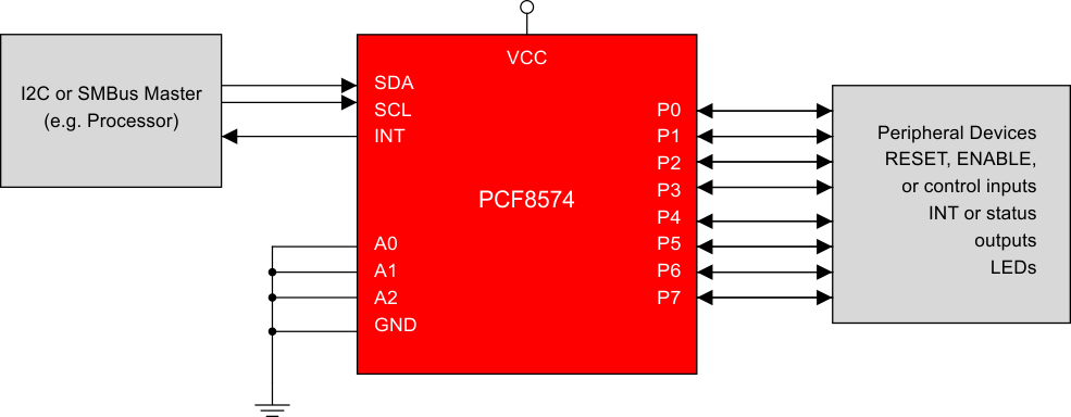
The PCF8574 device provides general-purpose remote I/O expansion for most microcontroller families by way of the I2C interface [serial clock (SCL), serial data (SDA)].
The device features an 8-bit quasi-bidirectional I/O port (P0–P7), including latched outputs with high-current drive capability for directly driving LEDs. Each quasi-bidirectional I/O can be used as an input or output without the use of a data-direction control signal. At power on, the I/Os are high. In this mode, only a current source to VCC is active.
| PART NUMBER | PACKAGE (1) | PACKAGE SIZE(2) |
|---|---|---|
| PCF8574 | TVSOP (DGV, 20) | 5mm × 6.40mm |
| SOIC (DW, 16) | 10.3mm × 10.3mm | |
| PDIP (N, 16) | 19.3mm × 9.4mm | |
| TSSOP (PW,20) | 6.5mm × 6.4mm | |
| VQFN (RGT, 16) | 3mm × 3mm | |
| VQFN (RGY, 20) | 4.5mm × 3.5mm |
 Simplified Schematic