SCPS178C July 2007 – April 2022 PCA9306-Q1
PRODUCTION DATA
- 1 Features
- 2 Applications
- 3 Description
- 4 Revision History
- 5 Description (continued)
- 6 Pin Configuration and Functions
-
7 Specifications
- 7.1 Absolute Maximum Ratings
- 7.2 ESD Ratings
- 7.3 Recommended Operating Conditions
- 7.4 Thermal Information
- 7.5 Electrical Characteristics
- 7.6 Switching Characteristics: Translating Down, VIH = 3.3 V
- 7.7 Switching Characteristics: Translating Down, VIH = 2.5 V
- 7.8 Switching Characteristics: Translating Up, VIH = 2.3 V
- 7.9 Switching Characteristics: Translating Up, VIH = 1.5 V
- 7.10 Typical Characteristics
- 8 Parameter Measurement Information
-
9 Detailed Description
- 9.1
Overview
- 9.1.1 Definition of threshold voltage
- 9.1.2 Correct Device Set Up
- 9.1.3 Disconnecting a Target from the Main I2C Bus Using the EN Pin
- 9.1.4 Supporting Remote Board Insertion to Backplane with PCA9306-Q1
- 9.1.5 Switch Configuration
- 9.1.6 Controller on Side 1 or Side 2 of Device
- 9.1.7 LDO and PCA9306-Q1 Concerns
- 9.1.8 Current Limiting Resistance on VREF2
- 9.2 Functional Block Diagram
- 9.3 Feature Description
- 9.4 Device Functional Modes
- 9.1
Overview
- 10Application and Implementation
- 11Power Supply Recommendations
- 12Layout
- 13Device and Documentation Support
- 14Mechanical, Packaging, and Orderable Information
9.1.7 LDO and PCA9306-Q1 Concerns
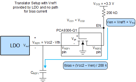
The VREF1 pin can be supplied by a low-dropout regulator (LDO), but in some cases the LDO can lose its regulation because of the bias current from VREF2 to VREF1. If the LDO cannot sink the bias current, then the current has no other paths to ground and instead charges up the capacitance on the VREF1 node (both external and parasitic). This results in an increase in voltage on the VREF1 node. If no other paths for current to flow are established (such as back biasing of body diodes or clamping diodes through other devices on the VREF1 node), then the VREF1 voltage ends up stabilizing when Vgs of the pass FET is equal to Vth. This means VREF1 node voltage is VCC2 - Vth. Note that any target or controllers running off of the LDO now see the VCC2 - Vth voltage which may cause damage to those target or controllers if they are not rated to handle the increased voltage.
 Figure 9-8 Example of no leakage current path when using LDO
To ensure LDO does not lose regulation due to the bias current of PCA9306-Q1, a weak pull down resistor can be placed on VREF1 to ground to provide a path for the bias current to travel. The recommended pull down resistor is calculated by Equation 4 where 0.75 gives about 25% margin for error incase bias current increases during operation.
 Figure 9-9 Example with Leakage current path when using an LDO
where
- Vth is approximately 0.6 V